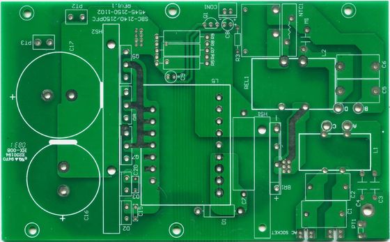

4OZ heavy copper pcb profession manufacturer thick board thickness
Material, FR4, RoHS compliance
Layer, 2Layer
Copper thickness, 4OZ heavey copper
Solder mask, Green
PCB Thickness, 1.6mm+/-10%
E-Test, 100%
Outgoing Reports, Final Inspection Report, E-Test Report, Solderability Test Report, Microsection Report and so on.
Inspection Standard, IPC-A-600H/IPC-6012B Class2 and IPC-A-600H/IPC-6012B class3
Certificates, UL, RoHS, ISO
PCB capability and services
1. Single-sided, double side and multi-layer PCB. FPC. Flex-Rigid PCB with competitive price, good quality and excellent service.
2. CEM-1, CEM-3 FR-4, FR-4 High TG, Aluminum base material, Polyimide, etc.
3. HAL, HAL lead free, Immersion Gold/ Silver/Tin, OSP surface treatment.
4. Printed Circuit Boards are 94V0 compliant, and adhere to IPC610 Class 2 international PCB standard.
5. Quantities range from Sample to mass order
6.100% E-Test
7. Qualified for CE and RoHS certificate
Feature
| Number of Layer | 1 - 20 Layer |
| Maximum Processing Area | 680 × 1000MM |
| Min Board Thickness | 2 Layer - 0.3MM ( 12 mil ) |
| 4 Layer - 0.4MM ( 16 mil ) | |
| 6 Layer - 0.8MM ( 32 mil ) | |
| 8 Layer - 1.0MM ( 40 mil) | |
| 10 Layer - 1.1MM ( 44 mil ) | |
| 12 Layer - 1.3MM ( 52 mil ) | |
| 14 Layer - 1.5MM ( 59 mil ) | |
| 16 Layer - 1.6MM ( 63 mil ) | |
| 18 Layer - 1.8MM ( 71 mil ) | |
| Finished Board Thickness Tolerance | Thickness ≤ 1.0MM, Tolerance: ± 0.1MM |
| 1.0MM ≤ Thickness ≤ 6.5MM, Tolerance ± 10% | |
| Twisting and Bending | ≤ 0.75%, Min: 0.5% |
| Range of TG | 130 - 215 ℃ |
| Impedance Tolerance | ± 10%, Min: ± 5% |
| Hi-Pot Test | Max: 4000V/10MA/60S |
| Surface Treatment | HASL, With Lead, HASL Free Lead |
| Flash Gold, Immersion Gold | |
| Immersion Silver, Immersion Tin | |
| Gold Finger, OSP |
PCBA capability and services SMT (Surface mounting technology), COB, DIP.
1. Material Sourcing Service
2. SMT assembly and Through hole components insertion
3. IC pre-programming / Burning on-line
4. Function testing as requested
5. Complete Unit assembly (which including plastics, metal box, Coil, cable inside etc)
6. OEM/ODM also welcomed
What we need
1. Gerber files of the bare PCB
2. Bill of materials to include: Manufacturer's part number, type of part, type of packaging, component locations listed by reference designators and quantity
3. Dimensional specifications for non-standard components
4. Assembly drawing, including any change notices
5. Final test procedures (if available)
Packing Terms
1. Inner packing. All the goods will be packed by vacuum
2. Outer packing. Standard carton
Quick Leadtime
Lead time for sample
2-3 days for single-sided board
4-5 days for double-sided board
6-7 days for multilayer board
24-48 hours for urgent
Lead time or opening Mould:
3-5 days for normal mould
5-7 days for hard mould
Lead time for mass production
5-7 days for single/double sided board
7-10 days for multilayer board