
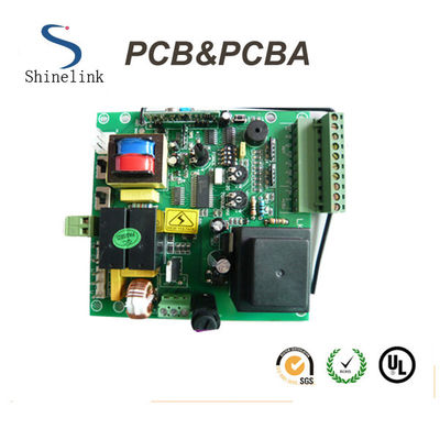
OEM and ODM turnkey pcb assembly for medical and industrial board
Our Service
1. PCB fabrication.
2. Turnkey PCBA, PCB + components + SMT, through-hole assembly + enclosure molding and housing
3. PCB clone, reverse engineering with all compoentns compeleted.
Our advantage
1. Free programming and free functional test, free package.
2. High quality. IPC-A-610E standard, E-test, X-ray, AOI test, QC, 100% funtional test.
3. Professional service. ISO SMT and through hole assembly, over 10 years experience.
4. Certification for electronics. UL, 94v-0, CE, SGS, FCC, RoHS, ISO9001:2008, ISO14001
5. Warranty period for PCBA. 2 years.
PCB Capacities and Technical Specification
| Order Quantity | 1-500,000 |
| Layer | 1,2,4,6,upto 18 layer |
| Material | FR-4,glass epoxy,FR4 High Tg,Rohs compliant,Aluminum,Rogers,etc |
| PCB type | Rigid,flexible,rigid-flexible |
| Shape | Any shape: Rectangular,round,slots,cutouts,complex,irregular |
| Max PCB dimensions | 20inch*20inch or 500mm*500mm |
| Thickness | 0.2~4.0mm, Flex 0.01~0.25'' |
| Thickness tolerance | ± 10% |
| Copper thickness | 0.5-4 oz |
| Copper thickness tolerance | ± 0.25oz |
| Surface finish | HASL,Nickle,Imm Gold,Imm Tin,Imm Silver,OSP etc |
| Solder mask | Green, red,white,yellow,blue,black, Double-sided |
| Silk screen | White,yellow,black,or negative, Double-sided or single-sided |
| Silk screen min line width | 0.006'' or 0.15mm |
| Min drill hole diameter | 0.01'',0.25mm.or 10 mil |
| Min trace/gap | 0.075mm or 3mil |
| PCB cutting | Shear,V-score,tab-routed |
PCBA Capabilities
| Turnkey PCBA | PCB+components sourcing+assembly+package |
| Assembly details | SMT and Thru-hole, ISO SMT and DIP lines |
| Lead Time | Prototype: 15 work days. Mass order: 20~25 work days |
| Testing on products | Flying Probe Test, X-ray Inspection, AOI Test, Functional test |
| Quantity | Min quantity: 1pcs. Prototype, small order, mass order, all OK |
| Files needed | PCB: Gerber files(CAM, PCB, PCBDOC) |
| Components: Bill of Materials(BOM list) | |
| Assembly: Pick-N-Place file | |
| PCB Panel Size | Min size: 0.25*0.25 inches(6*6mm) |
| Max size: 20*20 inches(500*500mm) | |
| PCB Solder Type | Water Soluble Solder Paste, RoHS lead free |
| Components details | Passive Down to 0201 size |
| BGA and VFBGA | |
| Leadless Chip Carriers/CSP | |
| Double-sided SMT Assembly | |
| Fine Pitch to 0.8mils | |
| BGA Repair and Reball | |
| Part Removal and Replacement | |
| Component package | Cut Tape,Tube,Reels,Loose Parts |
| PCB assembly process |
Drilling-----Exposure-----Plating-----Etaching & Stripping-----Punching-----Electrical Testing-----SMT-----Wave Soldering-----Assembling-----ICT-----Function Testing-----Temperature & Humidity Testing |
Packing details
Electronics PCBA are packed into plastic bags. Plastic bags are put into small carton. 4 small carton into a big carton.
Shipping Express
FedEx, DHL, UPS, TNT, EMS, private lines, etc.
Air freight, Sea shipping
Our products are sold all over the world, you can rest assured.
