Layout pcb prototype for oem medical devices with assembly service
Our PCB Requirements Need:
1. PCB board file with parts list provided by customers
2. PCB board made, circuit board parts purchased by us
3. PCB board with parts assembled
4. Electronic testing circuit board or PCBA
5. Fast delivery, anti-static package
6. RoHS Directive-compliant, lead-free
7. One stop service for PCB design, PCB layout, PCB manufacture, components purchasing, PCB assembly, test, packing and PCB delivery
PCB Capabilities
| Number of Layer | 1 - 20 Layer |
| Maximum Processing Area | 680 × 1000MM |
| Min Board Thickness | 2 Layer - 0.3MM ( 12 mil ) |
| 4 Layer - 0.4MM ( 16 mil ) | |
| 6 Layer - 0.8MM ( 32 mil ) | |
| 8 Layer - 1.0MM ( 40 mil) | |
| 10 Layer - 1.1MM ( 44 mil ) | |
| 12 Layer - 1.3MM ( 52 mil ) | |
| 14 Layer - 1.5MM ( 59 mil ) | |
| 16 Layer - 1.6MM ( 63 mil ) | |
| 18 Layer - 1.8MM ( 71 mil ) | |
| Finished Board Thickness Tolerance | Thickness ≤ 1.0MM, Tolerance: ± 0.1MM |
| 1.0MM ≤ Thickness ≤ 6.5MM, Tolerance ± 10% | |
| Twisting and Bending | ≤ 0.75%, Min: 0.5% |
| Range of TG | 130 - 215 ℃ |
| Impedance Tolerance | ± 10%, Min: ± 5% |
| Hi-Pot Test | Max: 4000V/10MA/60S |
| Surface Treatment | HASL, With Lead, HASL Free Lead |
| Flash Gold, Immersion Gold | |
| Immersion Silver, Immersion Tin | |
| Gold Finger, OSP |
FAQ
1. What service can you provide?
We can provide PCB circuit board gerber file design,Copy and Clone,OEM and ODM service.Not only produce PCB,PCB Assembly,but also Mold making ,Plastic Injection,and Complete products
2. Are my design files secure when I send them to you?
Your files are held in complete safety and security while Shinelink Technology Ltd is in possession of them. Your files are never shared nor will any third parties have access to your design files. Since they are your property, we respect the copyright of your files. The customer controls the disposition of these files per your requirements and written approval.
3. For small quantity orders, can you produce prototype PCBs?
Yes. Shinelink Technology Ltd has the capability to produce circuit boards in any amount. But,the greater the quantity, the greater the cost savings.
4. Do you have an order minimum?
We don't have MOQ, accept order with as low as a quantity of 1 (piece or panel).
5. What file formats do you accept for PCB assembly?
Gerber and CAM Auto CAD DXF, DWG formats.
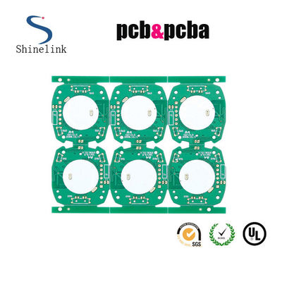
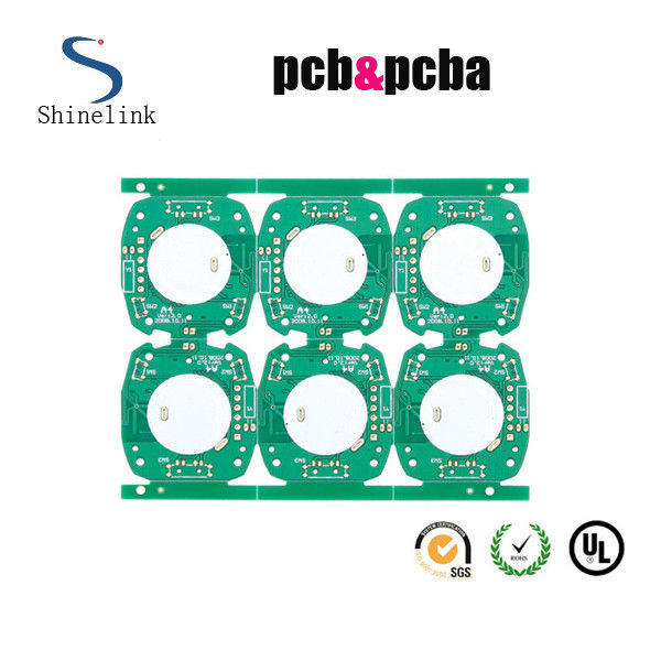
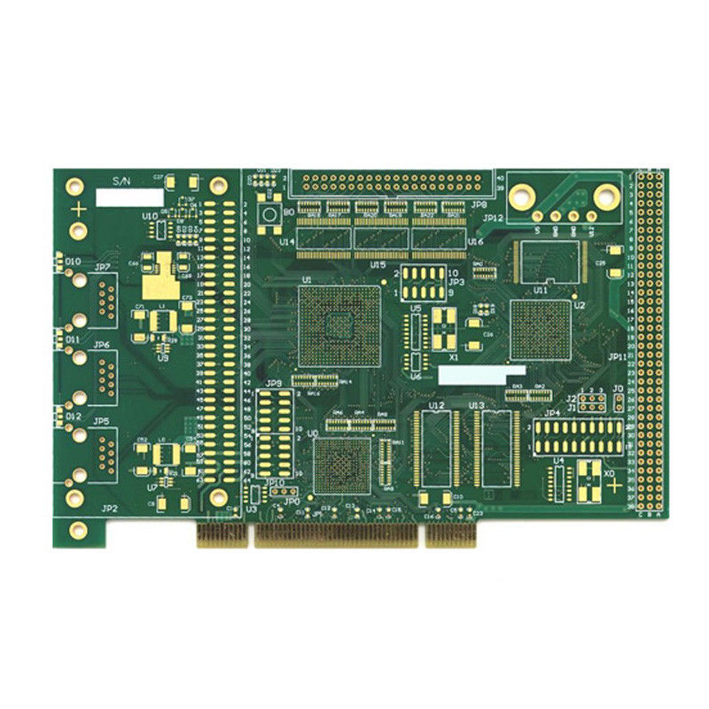
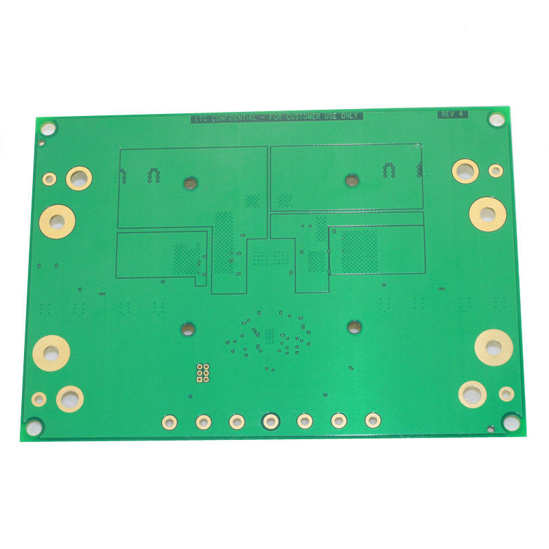
PCB Picture
![]()
Our products are sold all over the world, you can rest assured.