Electronic PCB manufacturer 100% AOI inspected 94v0 circuit board
Shinelink Company informaiton
Established in 2004, Shinelink company is a professional manufacturer of PCB & PCBA and EMS (electronics manufacturing service) with nearly 15-year experience in PCB Design & Layout, PCB Fabrication, PCB Assembly, PCBA Prototype, PCBA Test, Electronic Part Sourcing and EMS for kinds of smart electronic manufacturing.
PCB Manufacturing Lead Time.
| Layer/Days | Sample(Normal) | Sample(Fast) | Mass Production |
| Single/Double | 2-3days | 24hours | 5-7days |
| Four Layer | 7-10days | 3days | 7-10days |
| Six Layer | 7-10days | 5days | 13-15days |
| Eight Layer | 15-20days | 7days | 15-20days |
Reverse Engineering of Electronic PCB Assembly Manufacturing Products
We has developed capabilities of generating the necessary manufacturing documentation from finished
products. Services include.
1. Artwork and PCB Scanning
2. Schematics and Gerber File Generation
2. Bill of Material and Parts List Generation
PCB Assembly Capabilities
| Turnkey PCBA | PCB+components sourcing+assembly+package |
| Assembly details | SMT and Thru-hole, ISO lines |
| Lead Time | Prototype: 15 work days. Mass order: 20~25 work days |
| Testing on products | Flying Probe Test, X-ray Inspection, AOI Test, functional test |
| Quantity | Min quantity: 1pcs. Prototype, small order, mass order, all OK |
| Files we need | PCB: Gerber files(CAM, PCB, PCBDOC) |
| Components: Bill of Materials(BOM list) | |
| Assembly: Pick-N-Place file | |
| PCB panel Size | Min size: 0.25*0.25 inches(6*6mm) |
| Max size: 20*20 inches(500*500mm) | |
| PCB Solder Type | Water Soluble Solder Paste, RoHS lead free |
| Components details | Passive Down to 0201 size |
| BGA and VFBGA | |
| Leadless Chip Carriers/CSP | |
| Double-sided SMT Assembly | |
| Fine Pitch to 0.8mils | |
| BGA Repair and Reball | |
| Part Removal and Replacement | |
| Component package | Cut Tape,Tube,Reels,Loose Parts |
| PCB assembly process |
Drilling-----Exposure-----Plating-----Etaching & Stripping-----Punching-----Electrical Testing-----SMT-----Wave Soldering-----Assembling-----ICT-----Function Testing-----Temperature & Humidity Testing |
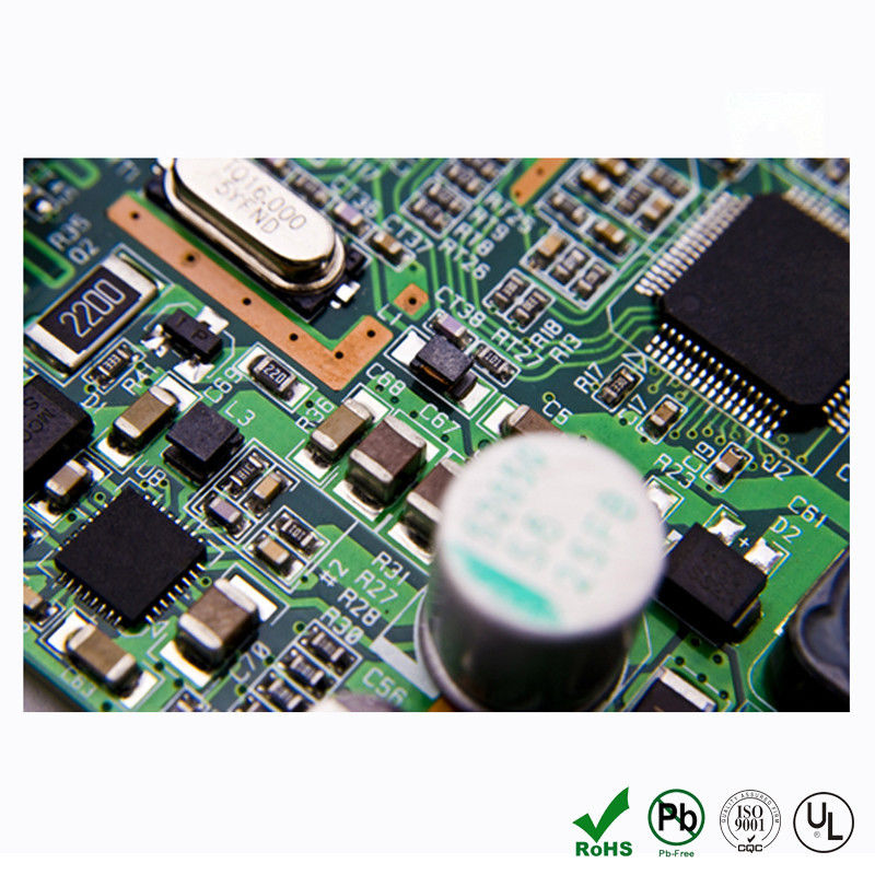
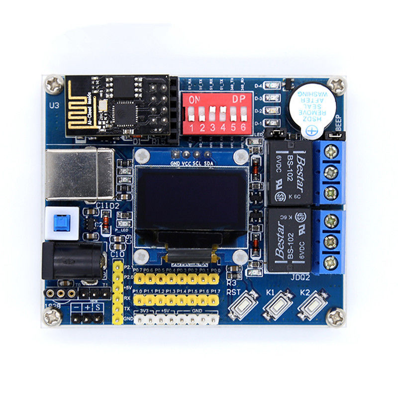
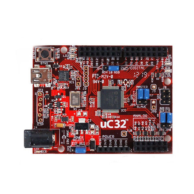
PCBA Picture
![]()
Our products are sold all over the world, you can rest assured.