High complexity PCB Prototype 1-18 layers Multilayers PCB RoHS 94v0
|
PCB Cu Thickness + Plating |
|
|
Out Layer Cu Thickness |
1 - 6OZ |
|
Inner Layer Cu Thickness |
0.5 - 4OZ |
|
Cu Thickness of PTH |
20UM ≤ Average ≤ 25UM |
|
Min: 18UM |
|
|
HASL with Lead |
Tin 63% Lead 37% |
|
HASL Free Lead |
7UM ≤ Surface Thickness ≤ 12UM |
|
Thick Gold Plating |
Ni Thickness: 3 - 5UM ( 120u" - 200u" ) |
|
Gold Thickness: 0.025 - 1.27UM ( 1u" - 50u" ) |
|
|
Immersion Gold |
Ni Thckness: 3 - 5UM ( 120u" - 200u" ) |
|
Gold Thickness: 0.025 - 0.15UM ( 1u" - 3u" ) |
|
|
Immersion Silver |
Ag Thickness: 0.15- 0.75 UM ( 6u" - 30u" ) |
|
Gold Finger |
Ni Thickness: 3 - 5UM ( 120u" - 160u" ) |
|
Gold Thickness: 0.025 - 1.51UM ( 1u" - 60u" ) |
|
|
U940 PCB Pattern Limit Capability |
|
|
Min Width |
0.075MM ( 3 mil ) |
|
Min Trace |
0.075MM ( 3 mil ) |
|
Min Width of Ring ( Inner Layer ) |
0.15MM ( 6 mil ) |
|
Min Width of Ring ( Out Layer ) |
0.1MM ( 4 mil ) |
|
Min Solder Bridge |
0.1MM ( 4 mil ) |
|
Min Height of Legend |
0.7MM ( 28 mil ) |
|
Min Width of Legend |
0.15MM ( 6 mil ) |
Reference - Our Production Capability for Rigid PCB
1) Layer: 1-18 Layers
2) Board finished thickness: 0.21mm-7.0mm
3) Material: FR-4, CEM-1,CEM-3, High TG, FR4 Halogen Free,Rogers
4) Max. finished board size: 23 × 25 ( 580mm×900mm )
5) Min. drilled hole size: 3mil (0.075mm)
6) Min. Line width: 3mil (0.075mm)
Min.Line spacing:3mil (0.075mm)
7) Surface finish/treatment : HASL / HASL lead free,HAL, Chemical tin,Chemical Gold, Immersion Silver/Gold,OSP,Gold plating
8) Copper thickness: 0.5-7.0 OZ
9) Solder mask color: green/yellow/black/white/red/blue
10) Copper thickness in hole: >25.0 um (>1mil)
11)Inner packing: Vacuum packing / Plastic bag
Outer packing: Standard carton packing
12) Shape tolerance: ±0.13
Hole tolerance: PTH: ±0.076 NPTH: ±0.05
13) Certificate: UL, ISO 9001, ISO 14001
14) Special requirements: Buried and blind vias+controlled impedance +BGA
15) Profiling: Punching, Routing, V-CUT, Beveling
16) Provides OEM services to all sorts of printed circuit board assembly as well as electronic encased products
PCB Capacity
|
Item
|
Capability---Technology
|
|
Standard
|
IPC-A-610 E Class II-III
|
|
Laminate/Base Material
|
FR-4 / PI (FPC) / High TG FR-4 / Halogen Free material/Rogers/Arlon/
Taconic/Teflon/CEM-3/PTFE/Aluminum /BT
|
|
Layers
|
1-18
|
|
Finised inner/outer copper thickness
|
1-6 OZ
|
|
Board Thinkness
|
0.2-5.0mm
|
|
Min hole size
|
Mechanical hole: 0.15mm
|
|
Laser hole: 0.1mm
|
|
|
Min line width/space
|
0.075mm/0.075mm
|
|
Min line Gap
|
+/-10%
|
|
Aspect Ratio
|
12:1
|
|
Controlled Impedance
|
<= +/-10%
|
|
Solder Mask Color
|
Green,Blue,Black,White,Yellow,Red,Grey,Purple etc..
|
|
Outline profile
|
Rout/ V-cut/ Bridge/ Stamp hole
|
|
Surface treatment
|
HASL, HASL lead free, Immersion Gold,ENEPIG, Immersion Tin, Immersion Silver, Hard gold, Flash gold, OSP...
|
|
Tolerance of dimension size
|
+/-0.1mm
|
|
Capacity
|
35000sq/Month
|
|
CAM Capability
|
40 item
|
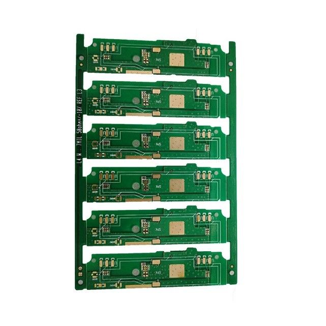
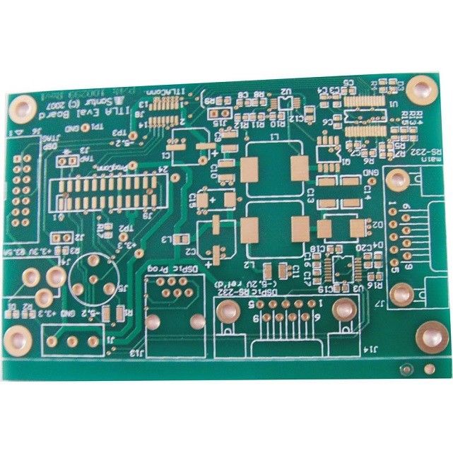
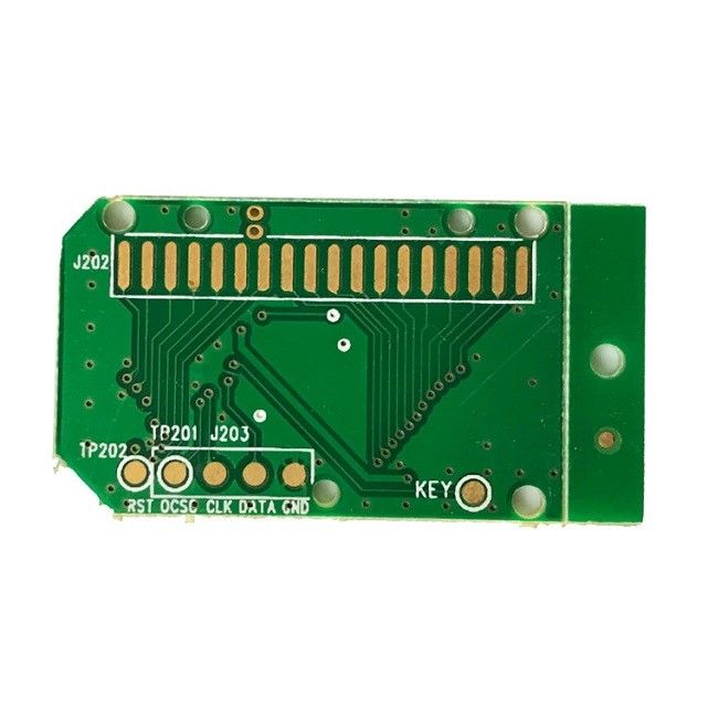
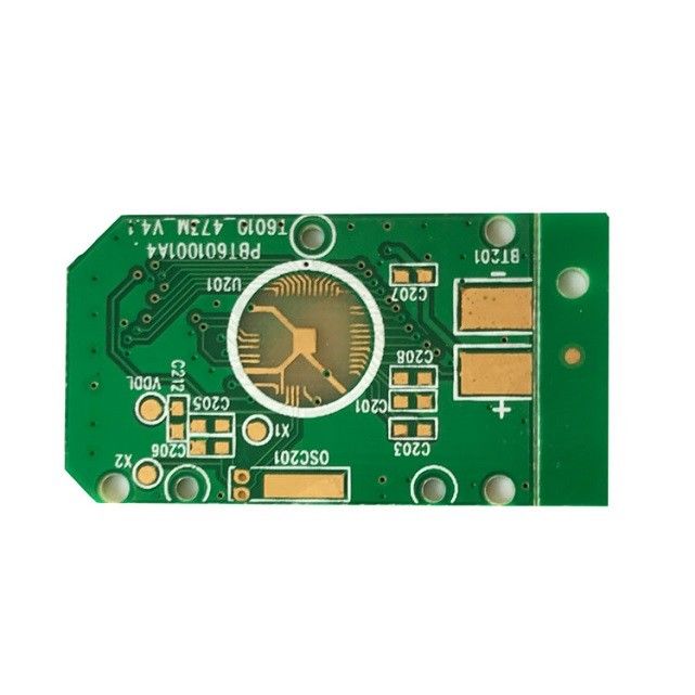
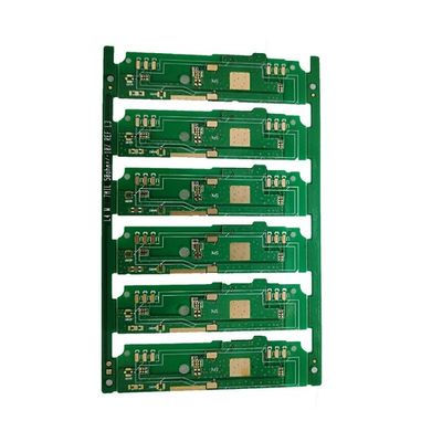
PCB Photos
![]()
![]()
Our products are sold all over the world, you can rest assured.