![]()
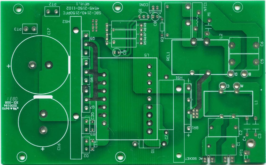
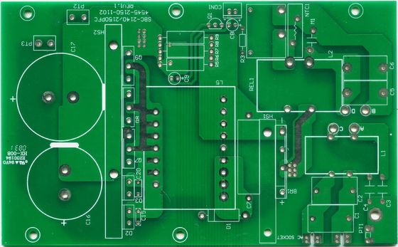
We are a Manufacturer & Supplier Specializing in Double Side PCB, Multi-Layer PCB, PTFE PCB, Ceramic PCB, Rogers PCB, Aluminium PCB, Flexible PCB with more than 10 years. Meanwhile, we provide PCBA ( Assembly) and ODM, OEM service. We are specializes in a full SMT and through hole PCBA assembly, obtaining components, building prototype quantities, and testing.
Our Production Capability for PCB
| Number of Layer | 1 - 20 Layer |
| Maximum Processing Area | 680 × 1000MM |
| Min Board Thickness | 2 Layer - 0.3MM ( 12 mil ) |
| 4 Layer - 0.4MM ( 16 mil ) | |
| 6 Layer - 0.8MM ( 32 mil ) | |
| 8 Layer - 1.0MM ( 40 mil) | |
| 10 Layer - 1.1MM ( 44 mil ) | |
| 12 Layer - 1.3MM ( 52 mil ) | |
| 14 Layer - 1.5MM ( 59 mil ) | |
| 16 Layer - 1.6MM ( 63 mil ) | |
| 18 Layer - 1.8MM ( 71 mil ) | |
| Finished Board Thickness Tolerance | Thickness ≤ 1.0MM, Tolerance: ± 0.1MM |
| 1.0MM ≤ Thickness ≤ 6.5MM, Tolerance ± 10% | |
| Twisting and Bending | ≤ 0.75%, Min: 0.5% |
| Range of TG | 130 - 215 ℃ |
| Impedance Tolerance | ± 10%, Min: ± 5% |
| Hi-Pot Test | Max: 4000V/10MA/60S |
| Surface Treatment | HASL, With Lead, HASL Free Lead |
| Flash Gold, Immersion Gold | |
| Immersion Silver, Immersion Tin | |
| Gold Finger, OSP |
Our PCBA Capability
SMT, PTH, mixed technology
SMT: 2,000,000 solder joints per day
DIP: 300,000 joints per day
Ultra fine pitch, QFP, BGA, μBGA, CBGA
Advanced SMT assembly
Automated insertion of PTH (axial, radial, dip)
Cleanable, aqueous and lead-free processing
RF manufacturing expertise
Peripheral process capabilities
Pressfit back planes & mid planes
Device programming
Automated conformal coating
For E-Test
Universal Tester
Flying Probe Open/Short Tester
High power Microscope
Solder ability Testing Kit
Peel Strength tester
High Volt Open & Short tester
Cross Section Molding Kit With Polisher
| If you need PCB assembly service as well, could you give us following information? | |
| 1. | Gerber file of the bare PCB board |
| 2. | BOM(Bill of material) for assembly |
| To short the Lead time, please kindly advise us if there is any acceptable components substitution. | |
| 3. | Testing Guide & Test Fixtures, if necessary |
| 4. | Programming files & Programming tool, is necessary |
| 5. | Schematic, if necessary |
![]()
![]()
![]()
![]()
![]()
Our products are sold all over the world, you can rest assured.