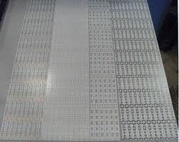

Multilayer Aluminum pcb board for LED grow light led bulb pcb
PCB Features
1. High quality products, Europoean and US standard
2. 3528 or 5050 SMD LED adopted,high brightness ,stable performance.
3. long lifetime,5% attenuation after 2500 hours,life time is 80000-100000 hours
4. Energy saving and environmental friendly.
5. 5m/rell is the standard package,but the size can be customized
6. Various of LED density optional, e.g.30LEDs/M,60LEDs/M,96LEDs/M. etc.
7. Each unit of 3LEDs can be cut out at regular segments.
8. White, warm white,red,green,blue and yellow color and RGB available.
Quote Requirements For PCB
1. Gerber File and Bom List;
2. Quote Quantity;
3. Technical requirements for quoting reference;
4. Clear pictures of PCB sample if available.
Lead Time For Production Orders
| PCB classification | Sample lead time(days) | Mass production lead time(days) |
| Single sided PCB | 1~3 | 4~7 |
| Double sided PCB | 2~5 | 7~10 |
| Multilayer PCB | 7~8 | 10~15 |
PCB Capabilities
| Number of Layer | 1 - 20 Layer |
| Maximum Processing Area | 680 × 1000MM |
| Min Board Thickness | 2 Layer - 0.3MM ( 12 mil ) |
| 4 Layer - 0.4MM ( 16 mil ) | |
| 6 Layer - 0.8MM ( 32 mil ) | |
| 8 Layer - 1.0MM ( 40 mil) | |
| 10 Layer - 1.1MM ( 44 mil ) | |
| 12 Layer - 1.3MM ( 52 mil ) | |
| 14 Layer - 1.5MM ( 59 mil ) | |
| 16 Layer - 1.6MM ( 63 mil ) | |
| 18 Layer - 1.8MM ( 71 mil ) | |
| Finished Board Thickness Tolerance | Thickness ≤ 1.0MM, Tolerance: ± 0.1MM |
| 1.0MM ≤ Thickness ≤ 6.5MM, Tolerance ± 10% | |
| Twisting and Bending | ≤ 0.75%, Min: 0.5% |
| Range of TG | 130 - 215 ℃ |
| Impedance Tolerance | ± 10%, Min: ± 5% |
| Hi-Pot Test | Max: 4000V/10MA/60S |
| Surface Treatment | HASL, With Lead, HASL Free Lead |
| Flash Gold, Immersion Gold | |
| Immersion Silver, Immersion Tin | |
| Gold Finger, OSP |
Specification
1. Surface Treatment ---- HASL,Flash gold Immersion Gold/Nickle,OSP
2. Number of Layer ----- Single Sided , Two-sided and multilayer ,Special layer
3. Max. PCB Size ----- 600mm×500mm
4. PCB Thickness ----- 0.5-5.0mm
5. Copper Foil Thickness ----- H 1 2 3 4 6 10 (oz)
6. Insulating Layer Thickness ----- 50 75 100 125 150 (um)
7. Metal Base Type ----- Al (1100,5052,6061),Cu, Fe, Stainless Steel etc.
8. Metal Substrate ----- 0.5 0.8 1.0 1.2 1.5 2.0 3.0 3.2 (mm)
9. Shaping ----- Die PunchingStampingRouteV-Cut
10.Solder Mask Colour ----- GreenWhiteBlackRedYellow
11. The Minimum Letter Height ----- 0.8 (mm)
12. The Minimum Letter Line Width ----- 0.15 (mm)
13.The Minimum Line Width ----- 0.15 (mm)
14. The Minimum Line Spacing ----- 0.15 (mm)
15. The Minimum Hole Diameter ----- 0.5 (mm)
16. Special hole ----- Spot facing, ,cup hole
17. File Format ----- Gerberprotelpowerpcbactocad
Applications
1. Indoor out door decoration.
2. Architectural and boutique atmosphere lighting.
3. Back, concealed , channel letter lighting.
4. Emergency and security, advertisement sign lighting.
5. Holiday Decoration.
Specification
1. Surface Treatment ---- HASL,Flash gold Immersion Gold/Nickle,OSP
2. Number of Layer ----- Single Sided , Two-sided and multilayer ,Special layer
3. Max. PCB Size ----- 600mm×500mm
4. PCB Thickness ----- 0.5-5.0mm
5. Copper Foil Thickness ----- H 1 2 3 4 6 10 (oz)
6. Insulating Layer Thickness ----- 50 75 100 125 150 (um)
7. Metal Base Type ----- Al (1100,5052,6061),Cu, Fe, Stainless Steel etc.
8. Metal Substrate ----- 0.5 0.8 1.0 1.2 1.5 2.0 3.0 3.2 (mm)
9. Shaping ----- Die PunchingStampingRouteV-Cut
10.Solder Mask Colour ----- GreenWhiteBlackRedYellow
11. The Minimum Letter Height ----- 0.8 (mm)
12. The Minimum Letter Line Width ----- 0.15 (mm)
13.The Minimum Line Width ----- 0.15 (mm)
14. The Minimum Line Spacing ----- 0.15 (mm)
15. The Minimum Hole Diameter ----- 0.5 (mm)
16. Special hole ----- Spot facing, ,cup hole
17. File Format ----- Gerberprotelpowerpcbactocad
About us
Shinelink Technology Ltd is more than just a leading PCB manufacturer. We are capable of providing all PCB assembly needs inculding full turnkey and partial turnkey printed circuit board assembly services.
For full turn-key, we take care of the entire process, including preparation of Printed Circuit Boards, procurement of components, online order tracking, continuous monitoring of quality and final assembly. Whereas for partial turn-key, the customer can provide the PCBs and certain components, and the remaining parts will be handled by us.
We has modernized its PCB assembly services to offer a one-stop, turn-key PCB assembly service which includes parts, fabrication and assembly - reducing production costs while improving quality and convenience.
Our Pcba service include
1. PCB board file with parts list provided by customers
2. PCB board made, circuit board parts purchased by us
3. PCB board with parts assembled
4. Electronic testing circuit board or PCBA
5. Fast delivery, anti-static package
6. RoHS Directive-compliant, lead-free
7. One stop service for PCB design, PCB layout, PCB manufacture, components purchasing, PCB assembly, test, packing and PCB delivery