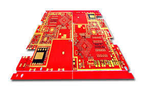
8 layer Heavy copper pcb Red soldermask with 5oz copper thickness
Brand Name: OEM
Material: FR4
Layer Count: 8 Layers
Board Thickness: 1.6 mm
Copper Thickness: 5OZ
Surface Finish: Lead Free Hasl
Solder Mask: Red(top&bot)
Silkscreen: White screen (top&bot)
Certification: UL, RoHS, ISO9001,
ISO14001, TS16949
Why choose Shinelink
1. Low cost PCB, you can save money on your prototype production.
2. Fast PCB prototype, PCB boards arrive your door only 8-10 days.
3. Prototype PCB, no min quantity required ,1pcs is OK!
4. Tooling charge only once, conducive to repeat order PCB Manufacture.
5. Quick Turn PCB, get detailed and exact quotation maybe only 1 hours.
6. Keep all costs to min and max our customers' benefits!
Quick Leadtime
Lead time for sample
2-3 days for single-sided board
4-5 days for double-sided board
6-7 days for multilayer board
24-48 hours for urgent
Lead time or opening Mould:
3-5 days for normal mould
5-7 days for hard mould
Lead time for mass production
5-7 days for single/double sided board
7-10 days for multilayer board
PCB Feature
| Number of Layer | 1 - 20 Layer |
| Maximum Processing Area | 680 × 1000MM |
| Min Board Thickness | 2 Layer - 0.3MM ( 12 mil ) |
| 4 Layer - 0.4MM ( 16 mil ) | |
| 6 Layer - 0.8MM ( 32 mil ) | |
| 8 Layer - 1.0MM ( 40 mil) | |
| 10 Layer - 1.1MM ( 44 mil ) | |
| 12 Layer - 1.3MM ( 52 mil ) | |
| 14 Layer - 1.5MM ( 59 mil ) | |
| 16 Layer - 1.6MM ( 63 mil ) | |
| 18 Layer - 1.8MM ( 71 mil ) | |
| Finished Board Thickness Tolerance | Thickness ≤ 1.0MM, Tolerance: ± 0.1MM |
| 1.0MM ≤ Thickness ≤ 6.5MM, Tolerance ± 10% | |
| Twisting and Bending | ≤ 0.75%, Min: 0.5% |
| Range of TG | 130 - 215 ℃ |
| Impedance Tolerance | ± 10%, Min: ± 5% |
| Hi-Pot Test | Max: 4000V/10MA/60S |
| Surface Treatment | HASL, With Lead, HASL Free Lead |
| Flash Gold, Immersion Gold | |
| Immersion Silver, Immersion Tin | |
| Gold Finger, OSP |
PCBA capability and services SMT (Surface mounting technology), COB, DIP.
1. Material Sourcing Service
2. SMT assembly and Through hole components insertion
3. IC pre-programming / Burning on-line
4. Function testing as requested
5. Complete Unit assembly (which including plastics, metal box, Coil, cable inside etc)
6. OEM/ODM also welcomed
Packing Terms
1. Inner packing. All the goods will be packed by vacuum
2. Outer packing. Standard carton
Our products are sold all over the world, you can rest assured.