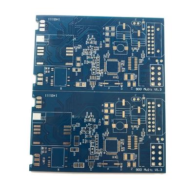

Gerber file multilayer pcb customed prototype printed circuit board
Multilayer PCB board
Shenzhen Shinelink Technology LTD. is a professional design company of printed circuit board and printed circuit board assembly manufacturing, dedicated to the Research ,Development,Production, Sales and Service of PCB and PCBA products for more than 14 years!
Advantages
- No MOQ
- OEM services provided
- Heavy copper PCB, Heavy gold PCB, Blind / Buried via PCB, High layer count PCB manufacturable
- Factory direct price
- Replying with price in one working day
- Shipping within 24 hours
- Certificate: ROHS, UL, ISO9001-2000, ISO14001,SGS Lead-Free
PCB Capacity
|
PCB General Capability |
|
|
Number of Layer |
1 - 18 Layer |
|
Maximum Processing Area |
680 × 1000MM |
|
Min Board Thickness |
2 Layer - 0.3MM ( 12 mil ) |
|
4 Layer - 0.4MM ( 16 mil ) |
|
|
6 Layer - 0.8MM ( 32 mil ) |
|
|
8 Layer - 1.0MM ( 40 mil) |
|
|
10 Layer - 1.1MM ( 44 mil ) |
|
|
12 Layer - 1.3MM ( 52 mil ) |
|
|
14 Layer - 1.5MM ( 59 mil ) |
|
|
16 Layer - 1.6MM ( 63 mil ) |
|
|
18 Layer - 1.8MM ( 71 mil ) |
|
|
Finished Board Thickness Tolerance |
Thickness ≤ 1.0MM, Tolerance: ± 0.1MM |
|
1.0MM ≤ Thickness ≤ 6.5MM, Tolerance ± 10% |
|
|
Twisting and Bending |
≤ 0.75%, Min: 0.5% |
|
Range of TG |
130 - 215 ℃ |
|
Impedance Tolerance |
± 10%, Min: ± 5% |
|
Hi-Pot Test |
Max: 4000V/10MA/60S |
|
Surface Treatment |
HASL, With Lead, HASL Free Lead |
|
Flash Gold, Immersion Gold |
|
|
Immersion Silver, Immersion Tin |
|
|
Gold Finger, OSP |
|
|
PCB Cu Thickness + Plating |
|
|
Out Layer Cu Thickness |
1 - 6OZ |
|
Inner Layer Cu Thickness |
0.5 - 4OZ |
|
Cu Thickness of PTH |
20UM ≤ Average ≤ 25UM |
|
Min: 18UM |
|
|
HASL with Lead |
Tin 63% Lead 37% |
|
HASL Free Lead |
7UM ≤ Surface Thickness ≤ 12UM |
|
Thick Gold Plating |
Ni Thickness: 3 - 5UM ( 120u" - 200u" ) |
|
Gold Thickness: 0.025 - 1.27UM ( 1u" - 50u" ) |
|
|
Immersion Gold |
Ni Thckness: 3 - 5UM ( 120u" - 200u" ) |
|
Gold Thickness: 0.025 - 0.15UM ( 1u" - 3u" ) |
|
|
Immersion Silver |
Ag Thickness: 0.15- 0.75 UM ( 6u" - 30u" ) |
|
Gold Finger |
Ni Thickness: 3 - 5UM ( 120u" - 160u" ) |
|
Gold Thickness: 0.025 - 1.51UM ( 1u" - 60u" ) |
|
|
U940 PCB Pattern Limit Capability |
|
|
Min Width |
0.075MM ( 3 mil ) |
|
Min Trace |
0.075MM ( 3 mil ) |
|
Min Width of Ring ( Inner Layer ) |
0.15MM ( 6 mil ) |
|
Min Width of Ring ( Out Layer ) |
0.1MM ( 4 mil ) |
|
Min Solder Bridge |
0.1MM ( 4 mil ) |
|
Min Height of Legend |
0.7MM ( 28 mil ) |
|
Min Width of Legend |
0.15MM ( 6 mil ) |
|
PCB Holes Processing Capability |
|
|
Final Hole Size |
Min: Laser 0.1MM, Machine 0.2MM |
|
Drilling Hole Size |
0.10 - 6.5MM |
|
Drilling Tolerance |
NPTH: ±0.05MM, PTH: ±0.075MM |
|
Final Hole Size Tolerance ( PTH ) |
φ0.20 - 1.60MM ± 0.075MM |
|
φ1.60 - 6.30MM ± 0.10MM |
|
|
Final Hole Size Tolerance ( NPTH ) |
φ0.20 - 1.60MM ± 0.05MM |
|
φ1.60 - 6.50MM ± 0.05MM |
|
|
Drilling Strip Hole |
-0L ~tu.'gth /width 2:1 |
|
Min Strip Hole Width 0.65MM |
|
|
Length & Width Tolerance ± 0.05MM |
|
|
Board Thickness / Hole Size |
≤ 10:1 |
|
PCB Cover Thickness Capability |
|
|
Solder Mask Color |
Green,Matte Green,Yellow,Blue,Red,Black,Matte Black,White |
|
Solder Mask Thickness |
Surface Line ≥ 10UM |
|
Surface Line Corner ≥ 6UM |
|
|
Surface Board 10 - 25UM |
|
|
Solder Mask Bridge Width |
|
|
Legend Color |
White,Yellow,Black |
|
Min Height of Legend |
0.70MM ( 28 mil ) |
|
Min Width of Legend |
0.15MM ( 6 mil ) |
|
Blue Gel Thickness |
0.2 - 1.5MM |
|
Blue Gel Tolerance |
±0.15MM |
|
Carbon Print Thickness |
5 - 25UM |
|
Carbon Print Min Space |
0.25MM |
|
Carbon Print Impedance |
200Ω |
|
Blind/Burried/Half Via PCB Capability |
|
|
Parameters |
(1+1)e.g. (4-layer)blind via:1-2,2-4 (6-layer)buried via:2-3,3-4 (8-layer)blind/buried:1-3,4-5,6-8 |
|
Min Via |
Laser 0.1MM, Machine 0.2MM |
|
Half Via |
Min: 0.6MM |
|
Impedance Capability |
|
|
Resistance Value |
Single-ended 50 - 75Ω, Difference 100Ω, Coplanar 50 - 75Ω |
PCB Photos
![]()
![]()