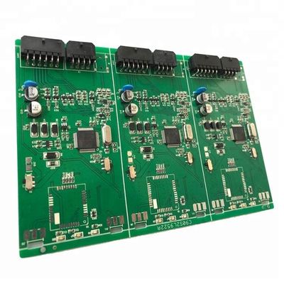
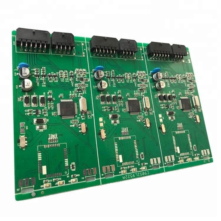
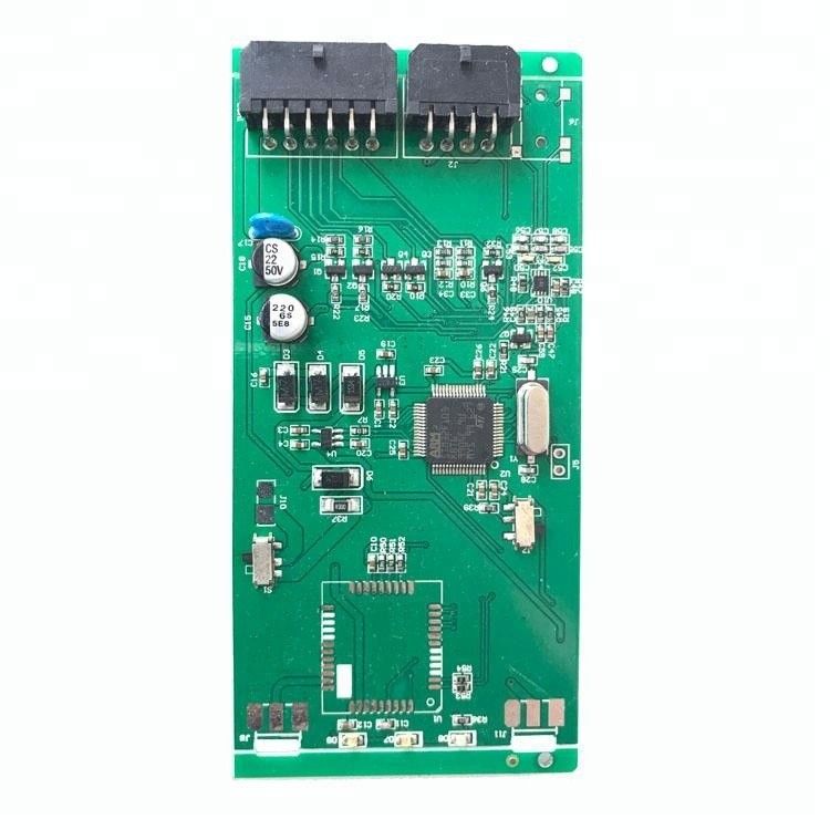
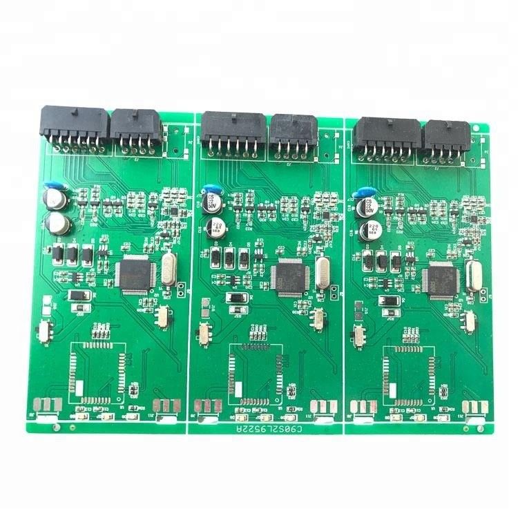
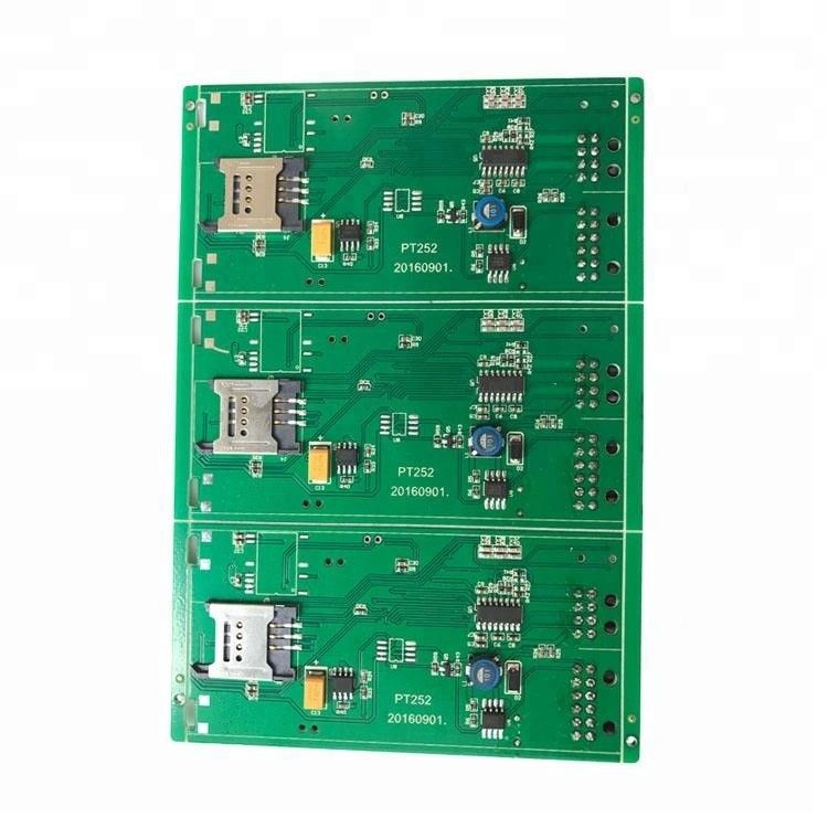
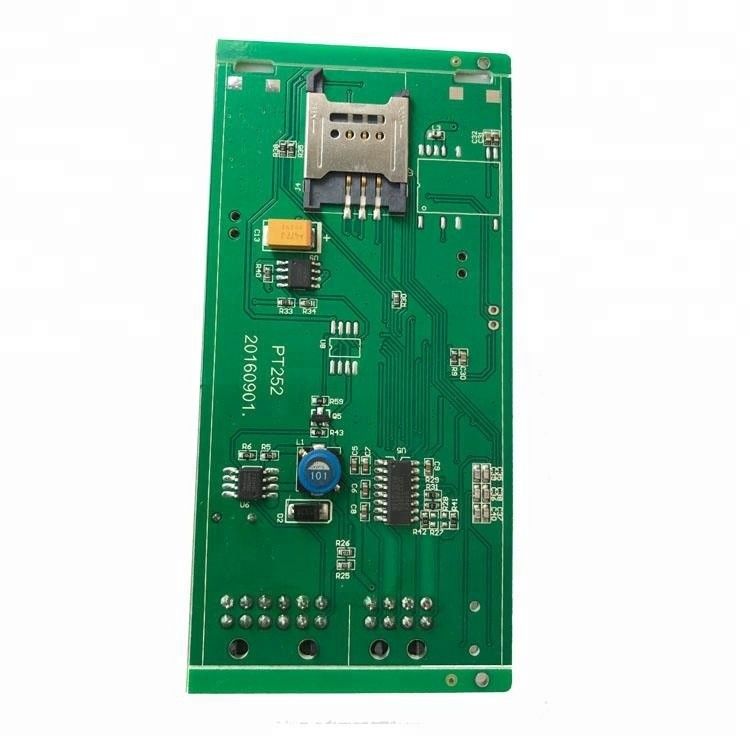
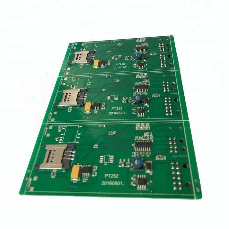
High Speed PCBA Board 2 Layer PCB Printed Board Assembly AOI Inspection
Turn-key service pcb assembly sample order have no MOQ. This PCBA assembly is with Leadfree Hasl surface treatment and multilayer design. The min. aperture is 0.075 mm. 94v0 fireproof help keep your product working well for the service term.
Files Requested For PCB Assembly Quotation
---In order to provide you with the most efficient and accurate quote on manufacturing the requested unit, we ask that you provide us with the following information.
1. Gerber file,PCB file,Eagle file or CAD file are all acceptable
2. A detailed bill of materials (BOM)
3. Clear pictures of PCB or PCBA sample for us
4. Quantity and delivery required
5. Test method for PCBA to guarantee 100% good quality products.
6. Schematics file for PCB design if need to do function test.
7. A sample if available for better sourcing
8. CAD files for enclosure manufacturing if required
9. A complete wiring and assembly drawing showing any special assembly instructions if required
Shinelink kinds PCBA product
![]()
94V0 PCBA manufacture Scale capabilities up to
We combine advanced processes with highly skilled resources. Keeping up with the leading advanced technology and management system in One-stop services of PCB assembly
SMT process (RoHs Compliant) Capabilities up to:
1. 0201 Chip Size
2. 12 mils Integrated Circuit (IC) Pitch
3. Micro Ball Grid Array (BGA) – Pitch 16 mils
4. Flip Chip (Controlled Collapse Chip Connection) – Pitch 5 mils
5. Quad Flat Package (QFP) – Pitch 12 mils
THT(Wave soldering) process (RoHs Compliant) Capabilities up to:
1.Single side wave soldering
2.SMT & THT mixture process
![]()
PCB Assembly Capabilities
|
Turnkey PCBA |
PCB+components sourcing+assembly+package |
|
Assembly details |
SMT and Thru-hole, ISO lines |
|
Lead Time |
Prototype: 15 work days. Mass order: 20~25 work days |
|
Testing on products |
Flying Probe Test, X-ray Inspection, AOI Test, functional test |
|
Quantity |
Min quantity: 1pcs. Prototype, small order, mass order, all OK |
|
Files we need |
PCB: Gerber files(CAM, PCB, PCBDOC) |
|
Components: Bill of Materials(BOM list) |
|
|
Assembly: Pick-N-Place file |
|
|
PCB panel Size |
Min size: 0.25*0.25 inches(6*6mm) |
|
Max size: 20*20 inches(500*500mm) |
|
|
PCB Solder Type |
Water Soluble Solder Paste, RoHS lead free |
|
Components details |
Passive Down to 0201 size |
|
BGA and VFBGA |
|
|
Leadless Chip Carriers/CSP |
|
|
Double-sided SMT Assembly |
|
|
Fine Pitch to 0.8mils |
|
|
BGA Repair and Reball |
|
|
Part Removal and Replacement |
|
|
Component package |
Cut Tape,Tube,Reels,Loose Parts |
|
PCB assembly |
Drilling-----Exposure-----Plating-----Etaching & Stripping-----Punching-----Electrical Testing-----SMT-----Wave Soldering-----Assembling-----ICT-----Function Testing-----Temperature & Humidity Testing |
PCBA Picture
![]()
![]()
Our products are sold all over the world, you can rest assured.