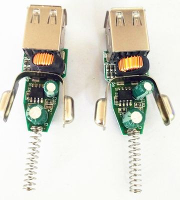

PCB assembly prototype service Electronic Circuit Board Turnkey RoHS
Shinelink company is an electronics manufacturing services (EMS) supplier located in Shenzhen, China. We provide customers with flexible and
reliable electronic manufacturing services, including parts procurement, circuit board processing, DIP, through-hole soldering, PCBA testing, box assembly, packaging and logistics.
PCB or PCB Assembly files requests
1. Gerber files of the bare PCB board
2. BOM (Bill of material) for assembly
To short the lead time, please kindly advise us if there is any acceptable components substitution.
3. Testing Guide & Test Fixtures if necessary
4. Programming files & Programming tool if necessary
5. Schematic if necessary
1.Bare Printed Circuit Board process capability:
| 1 | Layers | Single Sided,2 to 20 Layer |
| 2 | Board material type | FR4,CEM-1,CEM-3,ceramic substrate board, aluminum based board, high-Tg, Rogers and more |
| 3 | Compound material lamination | 4 to 6 layers |
| 4 | Maximum dimension | 610 x 1,100mm |
| 5 | Dimension tolerance | ±0.13mm |
| 6 | Board thickness coverage | 0.2 to 6.00mm |
| 7 | Board thickness tolerance | ±10% |
| 8 | DK thickness | 0.076 to 6.00mm |
| 9 | Minimum line width | 0.10mm |
| 10 | Minimum line space | 0.10mm |
| 11 | Outer layer copper thickness | 8.75 to 175µm |
| 12 | Inner layer copper thickness | 17.5 to 175µm |
| 13 | Drilling hole diameter (mechanical drill) | 0.25 to 6.00mm |
| 14 | Finished hole diameter (mechanical drill) | 0.20 to 6.00mm |
| 15 | Hole diameter tolerance (mechanical drill) | 0.05mm |
| 16 | Hole position tolerance (mechanical drill) | 0.075mm |
| 17 | Laser drill hole size | 0.10mm |
| 18 | Board thickness and hole diameter ratio | 10:1 |
| 19 | Solder mask type | Green, Yellow, Black, Purple, Blue, White and Red |
| 20 | Minimum solder mask | Ø0.10mm |
| 21 | Minimum size of solder mask separation ring | 0.05mm |
| 22 | Solder mask oil plug hole diameter | 0.25 to 0.60mm |
| 23 | Impedance control tolerance | ±10% |
| 24 | Surface finish | Hot air level, ENIG, immersion silver, gold plating, immersion tin and gold finger |
♦ All of the above description is to demonstrate the ability of our factory, if you have specific requirements, please contact us.
2.PCB (PCB Assembly) process capability:
| Technical Requirement | Professional Surface-mounting and Through-hole soldering Technology |
| Various sizes like 1206,0805,0603 components SMT technology | |
| ICT(In Circuit Test),FCT(Functional Circuit Test) technology | |
| PCB Assembly With UL,CE,FCC, RoHS Approval | |
| Nitrogen gas reflow soldering technology for SMT | |
| High Standard SMT&Solder Assembly Line | |
| High density interconnected board placement technology capacity | |
| Quote&Production Requirement | Gerber File or PCB File for Bare PCB Board Fabrication |
| BOM (Bill of Material) for Assembly,PNP (Pick and Place file) and Components Position also needed in assembly | |
| To reduce the quote time, please provide us the full part number for each components,Quantity per board also the quantity for orders. | |
| Testing Guide&Function Testing method to ensure the quality to reach nearly 0% scrap rate | |
| OEM/ODM/EMS Services | PCBA, PCB assembly: SMT & PTH & BGA |
| PCBA and enclosure design | |
| Components sourcing and purchasing | |
| Quick prototyping | |
| Plastic injection molding | |
| Metal sheet stamping | |
| Final assembly | |
| Test: AOI, In-Circuit Test (ICT), Functional Test (FCT) | |
| Custom clearance for material importing and product exporting | |
| Other PCB Assembly Equipment | SMT Machine: SIEMENS SIPLACE D1/D2 / SIEMENS SIPLACE S20/F4 |
| Reflow Oven: FL-RX860 | |
| Wave Soldering Machine: ADS300 | |
| Automated Optical Inspection (AOI): ALD-H-350B,X-RAY Testing Service | |
| Fully Automatic SMT Stencil Printer: Win-5 |