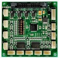
ODM custom smt circuit board assembly with 6 layers assembly service
About us
Shinelink Technology Ltd is more than just a leading PCB manufacturer. We are capable of providing all PCB assembly needs inculding full turnkey and partial turnkey printed circuit board assembly services.
For full turn-key, we take care of the entire process, including preparation of Printed Circuit Boards, procurement of components, online order tracking, continuous monitoring of quality and final assembly. Whereas for partial turn-key, the customer can provide the PCBs and certain components, and the remaining parts will be handled by us.
We has modernized its PCB assembly services to offer a one-stop, turn-key PCB assembly service which includes parts, fabrication and assembly - reducing production costs while improving quality and convenience.
Quote requirement:
Gerber file of the bare PCB board
BOM (bill of material) for assembly
To short the lead time, please kindly advise us if there is any acceptable components substitution
Testing guide and test fixtures if necessary
Programming files and programming tool if necessary
Schematic if necessary
PCB capability and services:
1. Single-sided, double-sided & multi-layer PCB (up to 30 layers)
2. Flexible PCB (up to 10 layers)
3. Rigid-flex PCB (up to 8 layers)
4. CEM-1, CEM-3 FR-4, FR-4 High TG, Polyimide, Aluminum-based material.
5. HAL, HAL lead free, Immersion Gold/ Silver/Tin, Hard Gold, OSP surface treatment.
6. Printed Circuit Boards are 94V0 compliant, and adhere to IPC610 Class 2 international PCB standard.
7. Quantities range from prototype to volume production.
8. 100% E-Test
Detail PCBA Capability
| Turnkey PCBA | PCB+components sourcing+assembly+package |
| Assembly details | SMT and Thru-hole, ISO SMT and DIP lines |
| Lead Time | Prototype: 15 work days. Mass order: 20~25 work days |
| Testing on products | Flying Probe Test, X-ray Inspection, AOI Test, Functional test |
| Quantity | Min quantity: 1pcs. Prototype, small order, mass order, all OK |
| Files needed | PCB: Gerber files(CAM, PCB, PCBDOC) |
| Components: Bill of Materials(BOM list) | |
| Assembly: Pick-N-Place file | |
| PCB Panel Size | Min size: 0.25*0.25 inches(6*6mm) |
| Max size: 20*20 inches(500*500mm) | |
| PCB Solder Type | Water Soluble Solder Paste, RoHS lead free |
| Components details | Passive Down to 0201 size |
| BGA and VFBGA | |
| Leadless Chip Carriers/CSP | |
| Double-sided SMT Assembly | |
| Fine Pitch to 0.8mils | |
| BGA Repair and Reball | |
| Part Removal and Replacement | |
| Component package | Cut Tape,Tube,Reels,Loose Parts |
| PCB assembly process |
Drilling-----Exposure-----Plating-----Etaching & Stripping-----Punching-----Electrical Testing-----SMT-----Wave Soldering-----Assembling-----ICT-----Function Testing-----Temperature & Humidity Testing |
Our products are sold all over the world, you can rest assured.