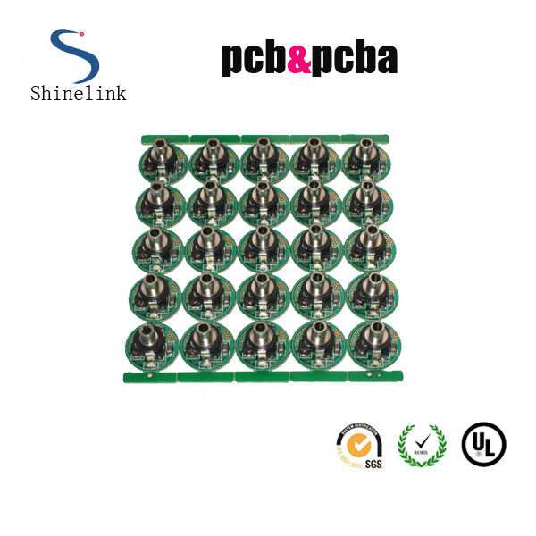
Power bank 2 layers pcb oem battery charger circuit diagram pcb
PCB capability and services
1. Single-sided, double side & multi-layer PCB. FPC. Flex-Rigid PCB with competitive price, good quality and excellent service.
2. CEM-1, CEM-3 FR-4, FR-4 High TG, Aluminum base material, Polyimide, etc.
3. HAL, HAL lead free, Immersion Gold/ Silver/Tin, OSP surface treatment.
4. Printed Circuit Boards are 94V0 compliant, and adhere to IPC610 Class 2 international PCB standard.
5. Quantities range from Sample to mass order
6.100% E-Test
7. Qualified for CE and RoHS certificate
PCBA capability and services SMT (Surface mounting technology), COB, DIP.
1. Material Sourcing Service
2. SMT assembly and Through hole components insertion
3. IC pre-programming / Burning on-line
4. Function testing as requested
5. Complete Unit assembly (which including plastics, metal box, Coil, cable inside etc)
6. OEM/ODM also welcomed
Feature
| Number of Layer | 1 - 20 Layer |
| Maximum Processing Area | 680 × 1000MM |
| Min Board Thickness | 2 Layer - 0.3MM ( 12 mil ) |
| 4 Layer - 0.4MM ( 16 mil ) | |
| 6 Layer - 0.8MM ( 32 mil ) | |
| 8 Layer - 1.0MM ( 40 mil) | |
| 10 Layer - 1.1MM ( 44 mil ) | |
| 12 Layer - 1.3MM ( 52 mil ) | |
| 14 Layer - 1.5MM ( 59 mil ) | |
| 16 Layer - 1.6MM ( 63 mil ) | |
| 18 Layer - 1.8MM ( 71 mil ) | |
| Finished Board Thickness Tolerance | Thickness ≤ 1.0MM, Tolerance: ± 0.1MM |
| 1.0MM ≤ Thickness ≤ 6.5MM, Tolerance ± 10% | |
| Twisting and Bending | ≤ 0.75%, Min: 0.5% |
| Range of TG | 130 - 215 ℃ |
| Impedance Tolerance | ± 10%, Min: ± 5% |
| Hi-Pot Test | Max: 4000V/10MA/60S |
| Surface Treatment | HASL, With Lead, HASL Free Lead |
| Flash Gold, Immersion Gold | |
| Immersion Silver, Immersion Tin | |
| Gold Finger, OSP |
PCB Assembly Capabilities
| Turnkey PCBA | PCB+components sourcing+assembly+package |
| Assembly details | SMT and Thru-hole, ISO lines |
| Lead Time | Prototype: 15 work days. Mass order: 20~25 work days |
| Testing on products | Flying Probe Test, X-ray Inspection, AOI Test, functional test |
| Quantity | Min quantity: 1pcs. Prototype, small order, mass order, all OK |
| Files we need | PCB: Gerber files(CAM, PCB, PCBDOC) |
| Components: Bill of Materials(BOM list) | |
| Assembly: Pick-N-Place file | |
| PCB panel Size | Min size: 0.25*0.25 inches(6*6mm) |
| Max size: 20*20 inches(500*500mm) | |
| PCB Solder Type | Water Soluble Solder Paste, RoHS lead free |
| Components details | Passive Down to 0201 size |
| BGA and VFBGA | |
| Leadless Chip Carriers/CSP | |
| Double-sided SMT Assembly | |
| Fine Pitch to 0.8mils | |
| BGA Repair and Reball | |
| Part Removal and Replacement | |
| Component package | Cut Tape,Tube,Reels,Loose Parts |
| PCB assembly process |
Drilling-----Exposure-----Plating-----Etaching & Stripping-----Punching-----Electrical Testing-----SMT-----Wave Soldering-----Assembling-----ICT-----Function Testing-----Temperature & Humidity Testing |
Advantage
1. ISO& UL certified third-party testing and high-quality technical service team.
2. Available and immediate delivery.
3. Producing capacity: 20,000sq meter/month.
4. Competitive price with no MOQ.
FAQ
1. What service can you provide?
We can provide PCB circuit board gerber file design,Copy and Clone,OEM and ODM service.Not only produce PCB,PCB Assembly,but also Mold making ,Plastic Injection,and Complete products
2. Are my design files secure when I send them to you?
Your files are held in complete safety and security while Shinelink Technology Ltd is in possession of them. Your files are never shared nor will any third parties have access to your design files. Since they are your property, we respect the copyright of your files. The customer controls the disposition of these files per your requirements and written approval.
3. For small quantity orders, can you produce prototype PCBs?
Yes. Shinelink Technology Ltd has the capability to produce circuit boards in any amount. But,the greater the quantity, the greater the cost savings.
4. Do you have an order minimum?
We don't have MOQ, accept order with as low as a quantity of 1 (piece or panel).
5. What file formats do you accept for PCB assembly?
Gerber and CAM Auto CAD DXF, DWG formats.
Our products are sold all over the world, you can rest assured.