High Volum PCB Assembly multilayer pcb manufacturing process
Shinelink PCBA is your source for fast affordable mid to high volume production runs of printed circuit board assemblies.we have over 15 years’ experience in PCB Assembly. We specialise in manufacturing mid to high-volume PCB assembly for the automotive, electronics, aviation and medical device industries.
Files Requested For PCB Assembly Quotation
---In order to provide you with the most efficient and accurate quote on manufacturing the requested unit, we ask that you provide us with the following information.
1. Gerber file,PCB file,Eagle file or CAD file are all acceptable
2. A detailed bill of materials (BOM)
3. Clear pictures of PCB or PCBA sample for us
4. Quantity and delivery required
5. Test method for PCBA to guarantee 100% good quality products.
6. Schematics file for PCB design if need to do function test.
7. A sample if available for better sourcing
8. CAD files for enclosure manufacturing if required
9. A complete wiring and assembly drawing showing any special assembly instructions if required
Shinelink PCBA’s PCB Assembly Services
Shinelink PCBA is a fully modern electronic manufacturing services (EMS) company. We offer the full range of services you need to assemble your printed circuit board, including:
Surface Mount Pick & Place Technology (SMT)
Through Hole Selective Soldering
Screen Solder Paste Printing or Jet Solder Paste Printing
Hand Solder & Assembly Services
Full Functional Test Capabilities
RoHS Bill of Material Conversions
Conformal Coating and Potting
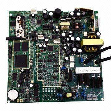
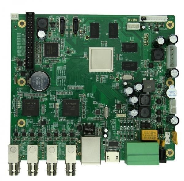
Shinelink kinds PCBA Products
![]()
Our PCB Manufacturing Capabilities
|
Types of PCB Assembly |
Surface Mount, Through Hole, Mixed Assemblies |
|
Lead or Lead Free |
|
|
Single or Double Sided |
|
|
No Clean Fluxes, Lead or Lead-free |
|
|
Programs |
Prototyping and Fast Turn |
|
Full Turnkey Assembly |
|
|
Consignment / Kanban / Order-Fulfillment Programs |
|
|
Labor Only / Customer Owned Components |
|
|
Components |
Passives parts, smallest size 01005 |
|
Fine pitch to 8 Mils |
|
|
BGA, uBGA, QFN, POP and Leadless chips |
|
|
Connectors and terminals |
|
|
Accepted Component Formats |
Reels, Digi-Reels |
|
Cut tape (allow leader or overage) |
|
|
Tube and tray |
|
|
Loose parts and bulk. Now offering reeling services. |
|
|
PCB Board shape |
Rectangular |
|
Round |
|
|
Slots and Cut outs |
|
|
Complex and Irregular |
|
|
PCB Board dimensions |
Smallest size: 1.2″ x 1.2″ (30 x 30 mm) |
|
Largest size: 15.1″ x 20″ (384 x 508 mm) |
|
|
Thickness Range: 0.02″ – 0.1875″ (0.5 – 4.76 mm) |
|
|
Clearances & Weights |
Board edge: 0.02″ – 0.14″ (0.5 – 3.5 mm) |
|
Top side: 0.50″ – 0.60″ (12.5 – 15 mm) |
|
|
Bottom side: 1.25″ (32 mm) |
|
|
Max board weight: 9lbs (4kg) |
|
|
PCB Board type |
Rigid FR-4, Rigid-Flex Boards |
|
Flexible, Flat-Flex (FFC) |
|
|
PCB Assembly process |
Leaded process |
|
Lead-Free (RoHS) |
|
|
Testing capabilities |
X-ray Inspection |
|
AOI (Automated Optical Inspection) |
|
|
ICT (In-Circuit Test) / Functional testing / Bed of Nails |
|
|
Design file format |
Gerber RS-274X |
|
BOM (Bill of Materials) (.xls, .csv, . xlsx) |
|
|
Centroid (Pick-N-Place/XY file) |
|
|
Oven profile |
Standard Reflow |
|
Custom Reflow |
|
|
Turnaround time |
1-5 days for only PCB assembly |
|
10-16 days for turnkey PCB assembly |
![]()
Our products are sold all over the world, you can rest assured.