HF PCB, High frequency printed circuit board for RF antenna Taconic
RF Antenna PCB information:
PCB Specification:
|
Layer of number |
4 |
Surface finish |
ENIG |
|
Base material |
Taconic |
Cu THK |
1OZ |
|
Board THK |
0.8mm |
Origin |
Shenzhen |
|
Board size |
12*6cm |
Solder mask |
Green |
Antenna pcb including:
GSM 3G antenna PCB, quad band antenna PCB, multil band antenna PCB,WIFI antenna pcb
Satellite antenna pcb, Car antenna pcb, GPS antenna pcb, GSM antenna pcb, Radar antenna pcb, FM/AM antenna pcb,2.4GHZ antenna pcb
We can offer production with high quality and competitive
|
Item |
Mass Production |
Pilot Run Production |
|
Capacity |
Capacity |
|
|
Layer Counts |
1L_18L, HDI |
20-28 , HDI |
|
Material |
FR4 |
|
|
Teflon,PTFE(F4B,F4BK), Rogers(4003,4350,5880) Taconic(TLX-8,TLX-9), Arlon(35N,85N)etc. |
||
|
Material Mixed Laminate |
4 layers -- 10 layers |
12 layers |
|
FR4+Ro4350 , Rogers3003+FR4 |
||
|
Maximum Size |
610mm X 1200mm |
1200 - 2000MM |
|
Board Outline Tolerance |
±0.15mm |
±0.10mm |
|
Board Thickness |
0.125mm--6.00mm |
0.1mm--8.00mm |
|
Thickness Tolerance ( t≥0.8mm) |
± 8% |
±5% |
|
Thickness Tolerance( t<0.8mm) |
±10% |
±8% |
|
Minimum Line / Space |
0.10mm |
0.075mm |
|
Trace width Tolerance |
15%-20% |
10% |
|
Minimum Drilling Hole (Mechanical) |
0.2mm |
0.15mm |
|
Minimum laser hole |
0.1mm |
0.075mm |
|
Hole Position/hole Tolerance |
±0.05mm PTH:±0.076MM NPTH:±0.05mm |
|
|
Mini hole ring (single |
0.075MM |
0.05MM |
|
OutLayer Copper Thickness |
17um--175um |
175um--210um |
|
InnerLayer Copper Thickness |
17um--175um |
175um--210um |
|
Mini Solder Mask Bridge |
0.05mm |
0.025mm |
|
Impedance Control Tolerance |
±10% |
±5% |
|
Surface Finishing |
HASL, Lead free HASL, Immersion gold, Immersion tin, Immersion Silver. |
|
|
Plated gold , OSP, Carbon ink, |
||
|
1-2L Lead-time |
3-7 days |
1-2 days |
|
4- 8L Lead-time |
7-10 days |
2-7 days |
|
10-18L Lead-time |
10-15 days |
4-9 days |
|
20-28L Lead-time |
15-20 days |
|
|
Acceptable File Format |
ALL Gerber Files,POWERPCB,PROTEL,PADS2000,CAD,AUTOCAD,ORCAD,P-CAD,CAM-350,CAM2000 etc. |
|
|
Quality Standards |
IPC-A-600F and MIL-STD-105D CHINA GB<4588> |
|
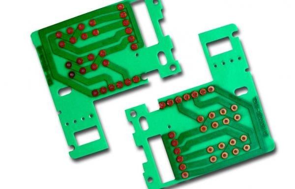
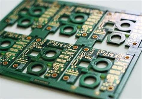
PCB Picture
![]()
Our products are sold all over the world, you can rest assured.