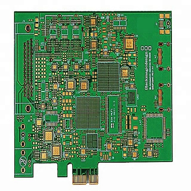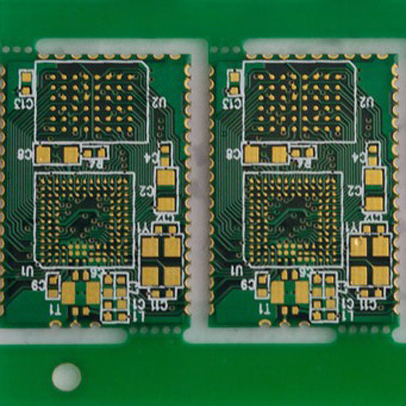
Rigid Multilayer PCB , High Density 8 Layer Immersion Gold PCB
8 layers PCBSpecification:
8-Layer Electronics 3 Oz Copper Base Multilayer Rigid PCB Security Electronics PCB
Green Soldermask White Silkscreen,
FR - 4 epoxy glass fiber cloth substrate, based on epoxy resin as binder,
with electronic level glass fiber cloth as reinforcing material of substrate.
Its bonding sheet and thin copper-clad r.p. panel and inner core is an important base material
in production of multilayer printed circuit board,
This kind of product is mainly used for double-sided PCB, dosage is very large.
Epoxy glass fiber cloth substrate, the most widely used model for FR - 4,
in recent years because of the electronic product installation technology
and PCB technology development needs, appeared high Tg FR - 4 products.
Advantage Highlights
Specialized in 2- to 32-layer PCB
ISO 9001-, ISO 14001- and ISO/TS 16949-certified
Products are UL- and RoHS-certified
Partner for over 2000 small- and medium-scale customers
Two factory bases totaling 22,000 square meters
Less than 12-hours quick response to inquiries
Widely acclaimed and satisfying services
Over 66% of PCBs are exported to international markets
Parameter:
|
|
Item |
Data |
|
1 |
Layer: |
1 to 18 layers |
|
2 |
Material type: |
FR-4, CEM-1, CEM-3, High TG, FR4 Halogen Free, Rogers |
|
3 |
Board thickness: |
0.20mm to 3.4mm |
|
4 |
Copper thickness: |
0.5 OZ to 4 OZ |
|
5 |
Copper thickness in hole: |
>25.0 um (>1mil) |
|
6 |
Max. Board Size: |
(580mm×1200mm) |
|
7 |
Min. Drilled Hole Size: |
4mil(0.1mm) |
|
8 |
Min. Line Width: |
3mil (0.075mm) |
|
9 |
Min. Line Spacing: |
3mil (0.075mm) |
|
10 |
Surface finishing: |
HASL / HASL lead free, HAL, Chemical tin, Chemical Gold, Immersion Silver/Gold, OSP, Gold plating |
|
11 |
Solder Mask Color: |
Green/Yellow/Black/White/Red/Blue |
|
12 |
Shape tolerance: |
±0.13 |
|
13 |
Hole tolerance: |
PTH: ±0.076 NPTH: ±0.05 |
|
14 |
Package: |
Inner packing: Vacuum packing / Plastic bag,Outer packing: Standard carton packing |
|
15 |
Certificate: |
UL,SGS,ISO 9001:2008 |
|
16 |
Special requirements: |
Buried and blind vias+controlled impedance +BGA |
|
17 |
Profiling: |
Punching, Routing, V-CUT, Beveling |
|
|
|
|
|
|
|
|
|
|
|
|
|
|
|
|
|
|
|
|
|
|
|
|
|
Green |
|
|
|
|
|
|
|
|
|
|
|
|
|
|
|
|
|
|
|
|
|
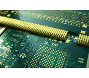
PCB Picture
![]()
Our products are sold all over the world, you can rest assured.