Thick copper 4OZ FR4 printed circuit board Prototype Immersion Tin / Silver
4OZ FR4 PCB Specifications
Thick copper printed circuit board
a). Impressive Quality
b). Fast Lead Time
c). Good Service
Thick copper printed circuit board
|
Process Capability |
||
|
|
||
|
|
||
|
ltem |
Mass Production |
Prototype |
|
|
||
|
Surface Treatment |
HASL(LF) |
HASL(LF) |
|
Immersion Gold |
Immersion Gold |
|
|
Flash Gold |
Flash Gold |
|
|
OSP |
OSP |
|
|
Immersion Tin |
Immersion Tin |
|
|
Immersion Silver |
Immersion Silver |
|
|
HASL&Gold Finger |
HASL&Gold Finger |
|
|
selective nickel |
selective nickel |
|
|
HASL(LF) |
smt Pad:>3um |
smt Pad:>4um |
|
Big Cu:>lum |
Big Cu:>l.5um |
|
|
Immersion Tin |
0.4-0.8um |
0.8-1.2um |
|
Immersion Gold |
Ni:2-5urn |
Ni:3-6urn |
|
Au:0.05-0.10um |
Au:0.075-0.15um |
|
|
Immersion Silver |
0.2-0.6um |
0.3-0.6um |
|
OSP |
0.1-0.4um |
0.25-0.4um |
|
Flash Gold |
Ni:3-6urn |
Ni:3-6urn |
|
Au:0.01-0.05um |
Au:0.02-0.075um |
|
|
Laminates |
CEM-3,PTFE |
CEM-3,PTFE |
|
FR4 (HighTG etc) |
FR4(HighTG etc) |
|
|
Metal Base(AL,CUetc) |
Metal Base(AL,CUetc) |
|
|
Rogors,etc |
Rogors,etc |
|
|
MAX.Layers |
12(Layers) |
40(Layers) |
|
MAX.Board Size |
20"X48" |
20"X48" |
|
Board Thickness |
O.4mm~6.0mm |
<O.4mm or >8.0mm |
|
Max.Copper Thickness |
inner Layer:16oz |
inner Layer:16oz |
|
Outer Layer:16oz |
Outer Layer:16oz |
|
|
Min.Track Width |
3mil/0.075mm |
3mil/0.075mm |
|
Min.Track Space |
3mil/0.075mm |
3mil/0.075mm |
|
M.in Hole Size |
8mil/0.2mm |
6mil/0.1mm |
|
M.in Laser Hole Size |
4mil/0.1mm |
3mil/0.076mm |
|
PTH Wall Thickness |
0.8mil/20um |
1.2mil/30um |
|
PTH Dia.Tolerance |
±2mil/±50um |
±2mil/±50um |
|
Aspect Ratio |
12:1 |
15:1 |
|
lmpedance Control |
±5% |
±5% |
PCBA Technology Capability
· Smallest chip placement:0201
· Automated axial insertion and Automated radial insertion
· Computer controlled Pb free wave soldering system
· High speed Pb free surface mount production lines
· Providing electronic components purchase service for the customers
· ICT on line inspection, PCBA function test equipment, Visual inspection
Mould And Box build Service
· Box Build
· Plastic injection
· Finish Packaging
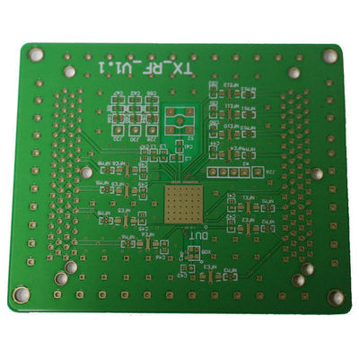
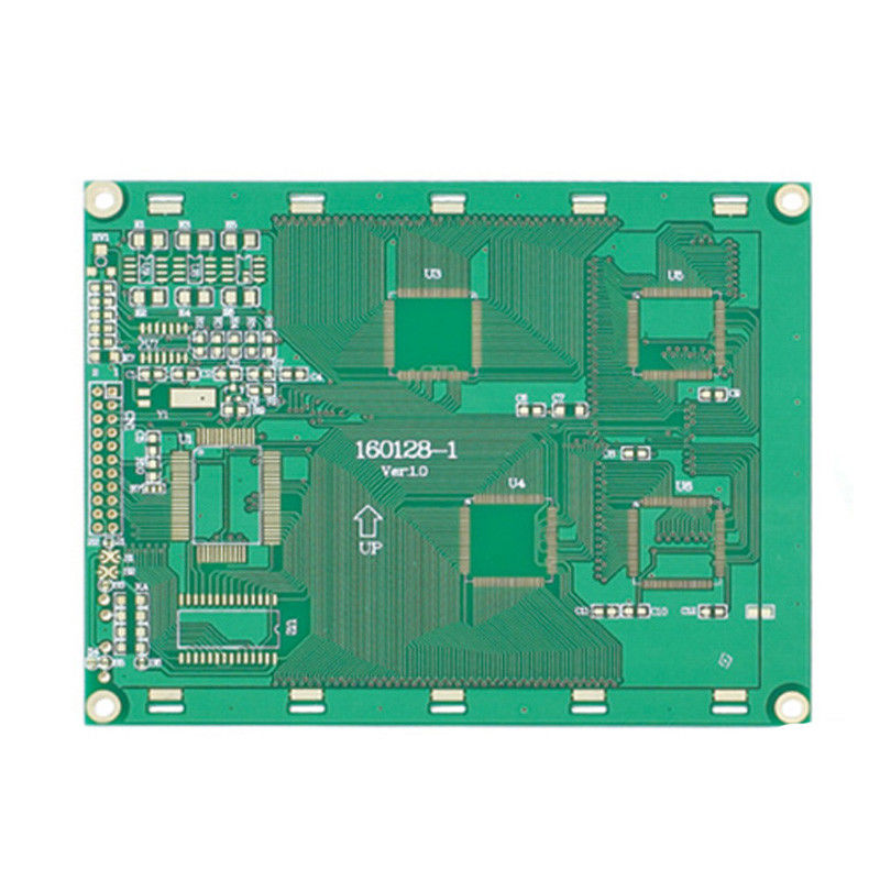
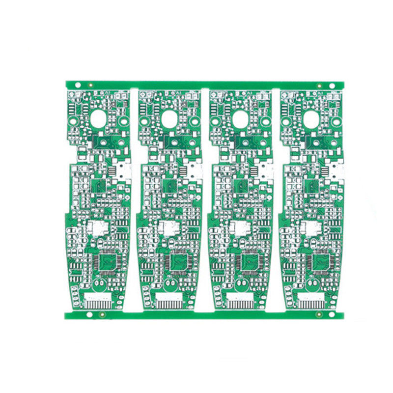
PCB Picture
![]()
Our products are sold all over the world, you can rest assured.