Small Volume Turnkey PCB Assembly 0.075mm Min Line Printed Circuit Board Manufacturing
PCB board manufacture and PCBA service:
* PCB board made, circuit board parts purchased by us
* Electronic testing circuit board or PCBA
* Fast delivery, anti-static package
* RoHS Directive-compliant, lead-free
* One stop service from PCB design, PCB layout, PCB manufacture, components purchasing, PCB assembly, test, packing and PCB delivery
* Electronic manufacturing service
SHINELINK, your single point of contact for all of your raw materials, parts, pcb assembly and finished product assembly, also offers
1. Contract Manufacturing
2. Engineering Services
3. PCB Design & Assembly
4. Product Design
5. Prototyping
6. Cable and Wire Assemblies
7. Plastics and Molds
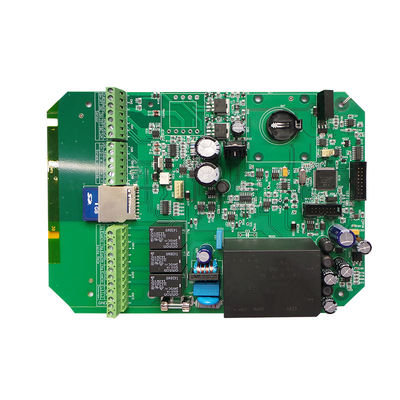
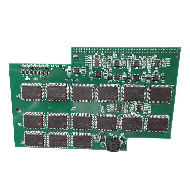
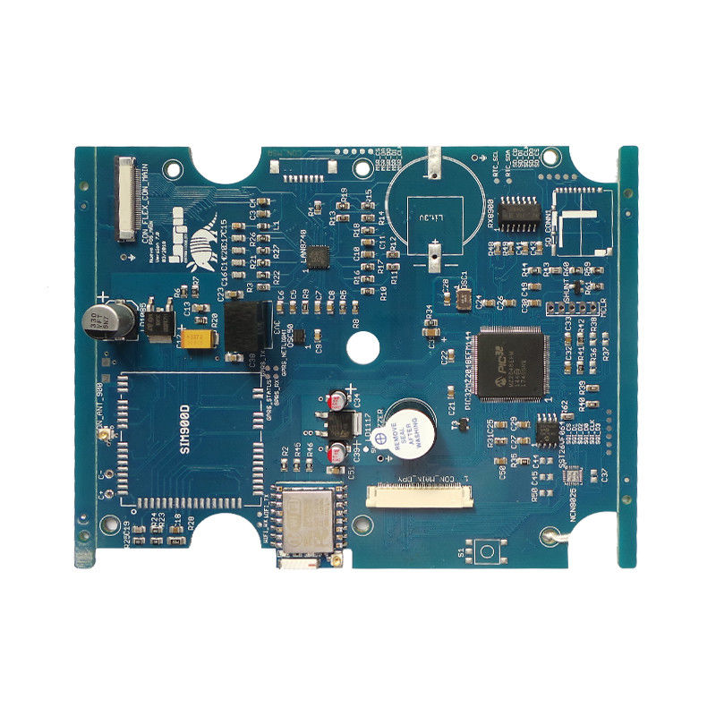
Shinelink kinds PCBA Products
![]()
Feature
| Number of Layer | 1 - 20 Layer |
| Maximum Processing Area | 680 × 1000MM |
| Min Board Thickness | 2 Layer - 0.3MM ( 12 mil ) |
| 4 Layer - 0.4MM ( 16 mil ) | |
| 6 Layer - 0.8MM ( 32 mil ) | |
| 8 Layer - 1.0MM ( 40 mil) | |
| 10 Layer - 1.1MM ( 44 mil ) | |
| 12 Layer - 1.3MM ( 52 mil ) | |
| 14 Layer - 1.5MM ( 59 mil ) | |
| 16 Layer - 1.6MM ( 63 mil ) | |
| 18 Layer - 1.8MM ( 71 mil ) | |
| Finished Board Thickness Tolerance | Thickness ≤ 1.0MM, Tolerance: ± 0.1MM |
| 1.0MM ≤ Thickness ≤ 6.5MM, Tolerance ± 10% | |
| Twisting and Bending | ≤ 0.75%, Min: 0.5% |
| Range of TG | 130 - 215 ℃ |
| Impedance Tolerance | ± 10%, Min: ± 5% |
| Hi-Pot Test | Max: 4000V/10MA/60S |
| Surface Treatment | HASL, With Lead, HASL Free Lead |
| Flash Gold, Immersion Gold | |
| Immersion Silver, Immersion Tin | |
| Gold Finger, OSP |
PCB Assembly Capabilities
| Turnkey PCBA | PCB+components sourcing+assembly+package |
| Assembly details | SMT and Thru-hole, ISO lines |
| Lead Time | Prototype: 15 work days. Mass order: 20~25 work days |
| Testing on products | Flying Probe Test, X-ray Inspection, AOI Test, functional test |
| Quantity | Min quantity: 1pcs. Prototype, small order, mass order, all OK |
| Files we need | PCB: Gerber files(CAM, PCB, PCBDOC) |
| Components: Bill of Materials(BOM list) | |
| Assembly: Pick-N-Place file | |
| PCB panel Size | Min size: 0.25*0.25 inches(6*6mm) |
| Max size: 20*20 inches(500*500mm) | |
| PCB Solder Type | Water Soluble Solder Paste, RoHS lead free |
| Components details | Passive Down to 0201 size |
| BGA and VFBGA | |
| Leadless Chip Carriers/CSP | |
| Double-sided SMT Assembly | |
| Fine Pitch to 0.8mils | |
| BGA Repair and Reball | |
| Part Removal and Replacement | |
| Component package | Cut Tape,Tube,Reels,Loose Parts |
| PCB assembly process |
Drilling-----Exposure-----Plating-----Etaching & Stripping-----Punching-----Electrical Testing-----SMT-----Wave Soldering-----Assembling-----ICT-----Function Testing-----Temperature & Humidity Testing |
![]()
Advantage
1. ISO& UL certified third-party testing and high-quality technical service team.
2. Available and immediate delivery.
3. Producing capacity: 20,000sq meter/month.
4. Competitive price with no MOQ.
FAQ:
1. How do Shinelink keep your price competitive?
Over the last decade, prices of many raw materials (e.g. copper, chemicals) had doubled, tripled or quadrupled; Chinese currency RMB had appreciated 31% over US dollar; And our labor cost also increased significantly.
However, Shinelink have kept our pricing steady. This owns entirely to our innovations in reducing cost, avoiding wastes and improving efficiency. Our prices are very competitive in the industry at the same quality level.
We believe in a win-win partnership with our customers. Our partnership will be mutually beneficial if we can provide you an edgeon cost and quality.
2. What kinds of boards can Shinelink process?
Common FR4, high-TG and halogen-free boards, Rogers, Arlon, Telfon, aluminum/copper-based boards, PI, etc.
3. What data are needed for PCB & PCBA production?
BOM (Bill of Materials) with reference designators: component description, manufacturer’s name and part number.
PCB Gerber files.
PCB fabrication drawing and PCBA assembly drawing.
Test procedures.
Any mechanical restrictions such as assembly height requirements.
4. What’s the typical process flow for multi-layer PCB?
Material cutting → Inner dry film → inner etching → Inner AOI → Multi-bond→ Layer stack up Pressing → Drilling → PTH → Panel Plating → Outer Dry Film → Pattern Plating → Outer etching → Outer AOI → Solder Mask → Component Mark → Surface finish → Routing → E/T → Visual Inspection.
Our products are sold all over the world, you can rest assured.