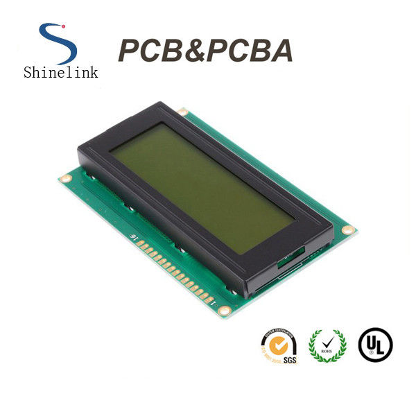
Rigid smt pcb assemlby for LCD module with advanced assembly
PCB Assembly services
SMT Assembly
Automatic Pick and Place
Component Placement as Small as 0201
Fine Pitch QEP - BGA
Automatic Optical Inspection
Through-hole Assembly
Wave Soldering
Hand Assembly and Soldering
Material Sourcing
IC pre-programming / Burning on-line
Function testing as requested
Aging test for LED and Power boards
Complete unit assembly (which including plastics, metal box, Coil, cable assembly etc)
Packing design
Our advantage
1. Free programming and free functional test, free package.
2. High quality. IPC-A-610E standard, E-test, X-ray, AOI test, QC, 100% funtional test.
3. Professional service. ISO SMT and through hole assembly, over 10 years experience.
4. Certification for electronics. UL, 94v-0, CE, SGS, FCC, RoHS, ISO9001:2008, ISO14001
5. Warranty period for PCBA. 2 years.
PCBA Capabilities
| Turnkey PCBA | PCB+components sourcing+assembly+package |
| Assembly details | SMT and Thru-hole, ISO SMT and DIP lines |
| Lead Time | Prototype: 15 work days. Mass order: 20~25 work days |
| Testing on products | Flying Probe Test, X-ray Inspection, AOI Test, Functional test |
| Quantity | Min quantity: 1pcs. Prototype, small order, mass order, all OK |
| Files needed | PCB: Gerber files(CAM, PCB, PCBDOC) |
| Components: Bill of Materials(BOM list) | |
| Assembly: Pick-N-Place file | |
| PCB Panel Size | Min size: 0.25*0.25 inches(6*6mm) |
| Max size: 20*20 inches(500*500mm) | |
| PCB Solder Type | Water Soluble Solder Paste, RoHS lead free |
| Components details | Passive Down to 0201 size |
| BGA and VFBGA | |
| Leadless Chip Carriers/CSP | |
| Double-sided SMT Assembly | |
| Fine Pitch to 0.8mils | |
| BGA Repair and Reball | |
| Part Removal and Replacement | |
| Component package | Cut Tape,Tube,Reels,Loose Parts |
| PCB assembly process |
Drilling-----Exposure-----Plating-----Etaching & Stripping-----Punching-----Electrical Testing-----SMT-----Wave Soldering-----Assembling-----ICT-----Function Testing-----Temperature & Humidity Testing |
Packing details
Electronics PCBA are packed into plastic bags. Plastic bags are put into small carton. 4 small carton into a big carton.
Shipping Express
FedEx, DHL, UPS, TNT, EMS, private lines, etc.
Air freight, Sea shipping
Our products are sold all over the world, you can rest assured.