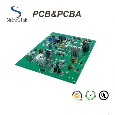
High Density PCB SMT Assembly wave soldering with function test PCBA
PCB capability and services:
1. Single-sided, double-sided & multi-layer PCB (up to 30 layers)
2. Flexible PCB (up to 10 layers)
3. Rigid-flex PCB (up to 8 layers)
4. CEM-1, CEM-3 FR-4, FR-4 High TG, Polyimide, Aluminum-based material.
5. HAL, HAL lead free, Immersion Gold/ Silver/Tin, Hard Gold, OSP surface treatment.
6. Printed Circuit Boards are 94V0 compliant, and adhere to IPC610 Class 2 international PCB standard.
7. Quantities range from prototype to volume production.
8. 100% E-Test
Our advantage
1. Free programming and free functional test, free package.
2. High quality. IPC-A-610E standard, E-test, X-ray, AOI test, QC, 100% funtional test.
3. Professional service. ISO SMT and through hole assembly, over 10 years experience.
4. Certification for electronics. UL, 94v-0, CE, SGS, FCC, RoHS, ISO9001:2008, ISO14001
5. Warranty period for PCBA. 2 years.
PCBA Capabilities
| Turnkey PCBA | PCB+components sourcing+assembly+package |
| Assembly details | SMT and Thru-hole, ISO SMT and DIP lines |
| Lead Time | Prototype: 15 work days. Mass order: 20~25 work days |
| Testing on products | Flying Probe Test, X-ray Inspection, AOI Test, Functional test |
| Quantity | Min quantity: 1pcs. Prototype, small order, mass order, all OK |
| Files needed | PCB: Gerber files(CAM, PCB, PCBDOC) |
| Components: Bill of Materials(BOM list) | |
| Assembly: Pick-N-Place file | |
| PCB Panel Size | Min size: 0.25*0.25 inches(6*6mm) |
| Max size: 20*20 inches(500*500mm) | |
| PCB Solder Type | Water Soluble Solder Paste, RoHS lead free |
| Components details | Passive Down to 0201 size |
| BGA and VFBGA | |
| Leadless Chip Carriers/CSP | |
| Double-sided SMT Assembly | |
| Fine Pitch to 0.8mils | |
| BGA Repair and Reball | |
| Part Removal and Replacement | |
| Component package | Cut Tape,Tube,Reels,Loose Parts |
| PCB assembly process |
Drilling-----Exposure-----Plating-----Etaching & Stripping-----Punching-----Electrical Testing-----SMT-----Wave Soldering-----Assembling-----ICT-----Function Testing-----Temperature & Humidity Testing |
FAQ
1. What service can you provide?
We can provide PCB circuit board gerber file design,Copy and Clone,OEM and ODM service.Not only produce PCB,PCB Assembly,but also Mold making ,Plastic Injection,and Complete products
2. Are my design files secure when I send them to you?
Your files are held in complete safety and security while Shinelink Technology Ltd is in possession of them. Your files are never shared nor will any third parties have access to your design files. Since they are your property, we respect the copyright of your files. The customer controls the disposition of these files per your requirements and written approval.
3. For small quantity orders, can you produce prototype PCBs?
Yes. Shinelink Technology Ltd has the capability to produce circuit boards in any amount. But,the greater the quantity, the greater the cost savings.
4. Do you have an order minimum?
We don't have MOQ, accept order with as low as a quantity of 1 (piece or panel).
5. What file formats do you accept for PCB assembly?
Gerber and CAM Auto CAD DXF, DWG formats.
Our products are sold all over the world, you can rest assured.