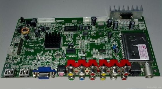
Double sided smt pcb assembly, printed circuit board assembly
Advantage
1. Turnkey manufacturing or quick-turn prototypes
2. Board-level assembly or complete system integration
3. Low-volume or mixed-technology assembly for PCBA
4. Even consignment production
5. Supported capabilities
Type of assembly
1. THD (thru-hole device)/conventional
2. SMT (surface-mount technology)
3. SMT and THD mixed
4. Double-sided SMT and/or THD assembly
Quote requirement:
Gerber file of the bare PCB board
BOM (bill of material) for assembly
To short the lead time, please kindly advise us if there is any acceptable components substitution
Testing guide and test fixtures if necessary
Programming files and programming tool if necessary
Schematic if necessary
PCB capability and services:
1. Single-sided, double-sided & multi-layer PCB (up to 30 layers)
2. Flexible PCB (up to 10 layers)
3. Rigid-flex PCB (up to 8 layers)
4. CEM-1, CEM-3 FR-4, FR-4 High TG, Polyimide, Aluminum-based material.
5. HAL, HAL lead free, Immersion Gold/ Silver/Tin, Hard Gold, OSP surface treatment.
6. Printed Circuit Boards are 94V0 compliant, and adhere to IPC610 Class 2 international PCB standard.
7. Quantities range from prototype to volume production.
8. 100% E-Test
Detail PCBA Capability
| Turnkey PCBA | PCB+components sourcing+assembly+package |
| Assembly details | SMT and Thru-hole, ISO SMT and DIP lines |
| Lead Time | Prototype: 15 work days. Mass order: 20~25 work days |
| Testing on products | Flying Probe Test, X-ray Inspection, AOI Test, Functional test |
| Quantity | Min quantity: 1pcs. Prototype, small order, mass order, all OK |
| Files needed | PCB: Gerber files(CAM, PCB, PCBDOC) |
| Components: Bill of Materials(BOM list) | |
| Assembly: Pick-N-Place file | |
| PCB Panel Size | Min size: 0.25*0.25 inches(6*6mm) |
| Max size: 20*20 inches(500*500mm) | |
| PCB Solder Type | Water Soluble Solder Paste, RoHS lead free |
| Components details | Passive Down to 0201 size |
| BGA and VFBGA | |
| Leadless Chip Carriers/CSP | |
| Double-sided SMT Assembly | |
| Fine Pitch to 0.8mils | |
| BGA Repair and Reball | |
| Part Removal and Replacement | |
| Component package | Cut Tape,Tube,Reels,Loose Parts |
| PCB assembly process |
Drilling-----Exposure-----Plating-----Etaching & Stripping-----Punching-----Electrical Testing-----SMT-----Wave Soldering-----Assembling-----ICT-----Function Testing-----Temperature & Humidity Testing |
Our products are sold all over the world, you can rest assured.