Substrate fr4 pcb prototype circuit board multilayer 4 layers No MOQ
Substrate fr4 pcb prototype Specifications
Substrate fr4 printed circuit board
1. High quality board
2. Quick turn
3. Strong engineering surpport
4. SGS,ISO,UL,ROHS,IPC
|
Production Description
|
-
specialized in single-sided PCB, double-sided PCB, multilayer PCB and PCBA.
-
Material Type: FR4,CEM-1,non-halogen,Aluminium, high frequency, 94-V0, PI, High TG
-
Surface treatment: HASL, LF, Immersion Gold, Immersion Tin/ silver, Gold Finger, OSP
|
|
|
|
|
|
|
Item
|
Capabilities
|
|
1.Base Material
|
FR-4 / High TG FR-4 / Lead free Materials (ROHS Compliant) /
Halogen Free material /CEM-3/CEM-1/ /PTFE/ROGERS/ARLON/TACONIC
|
|
2.Layers
|
1-30
|
|
3.Finised inner/outer copper thickness
|
1-12OZ
|
|
4.Finished board thickness
|
0.2-7.0mm
|
|
Tolerance
|
Board thickness≤1.0mm: +/-0.1mm
1<Board thickness≤2.0mm: +/-10%
Board thickness>2.0mm: +/-8%
|
|
5.Max panel size
|
≤2sidesPCB: 600*1500mm
Multilayer PCB: 500*1200mm
|
|
6.Min conductor line width/spacing
|
Inner layers: ≥3/3mil
Outer layers: ≥3.5/3.5mil
|
|
7.Min hole size
|
Mechanical hole: 0.2mm
Laser hole: 0.1mm
|
|
Drilling precision: first drilling
|
First drilling: 1mil
Second drilling: 4mil
|
|
8.Warpage
|
Board thickness≤0.79mm: β≤1.0%
0.80≤Board thickness≤2.4mm: β≤0.7%
Board thickness≥2.5mm: β≤0.5%
|
|
9.Controlled Impedance
|
+/-5%
|
|
10. Aspect Ratio
|
15:1
|
|
11.Min welding ring
|
4mil
|
|
12.Min solder mask bridge
|
≥0.08mm
|
|
13.Plugging vias capability
|
0.2-0.8mm
|
|
14. Hole tolerance
|
PTH: +/-3mil
NPTH: +/-2mil
|
|
15.Outline profile
|
Rout/ V-cut/ Bridge/ Stamp hole
|
|
16.Surface treatment
|
OSP: 0.5-0.5um
HASL: 2-40um
Lead free HASL: 2-40um
ENIG: Au 1-10U’’
ENEPIG: PB 2-5U’’/ Au 1-8U’’
Immersion Tin:0.8-1.2um
Immersion silver: 0.1-1.2um
Peelable blue mask
Carbon ink
Gold plating: Au 1-150U’’
|
|
17. E-testing pass percent
|
97% pass for the first time,+/-2%(tolerance)
|
|
FQC-Physical Lab: Reliability tests
|
|
18.Certificate
|
ROHS UL ISO9001:2008 IPC SGS
|
|
|
|
Our equipments
|
|
1.Drilling workshop
|
4 drilling bits of drilling machine: 4 sets
2 drilling bits of drilling machine: 2 sets
|
|
2. photo plotting workshop
|
Israel “ORBOTECH” Photo Plotters
|
|
3.AOI
|
AOI machine
|
|
4.IPQC
|
“OXFORD” CMI 700 Copper Thickness Tester
|
|
5.Impedance test
|
USA “Tektronix” DSA 8200 Impedance Tester
|
|
6.Outline workshop
|
CNC routing machine: 7 sets
angle-cutting machine
V-cut machine
|
|
7.Testing Workshop
|
Surpass X-600: 2sets
WTD FT-2808: 5sets
WTD HV300: 1set
|
|
8.X-ray
|
X-ray machine
|
|
|
|
Acceptable file format
|
|
GERBER file, PROTEL series, PADS series, POWER PCB series, AutoCAD series.
|
|
|
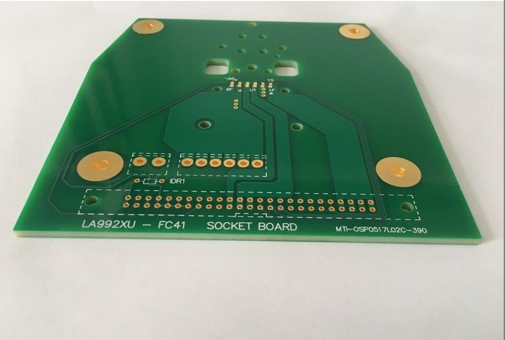
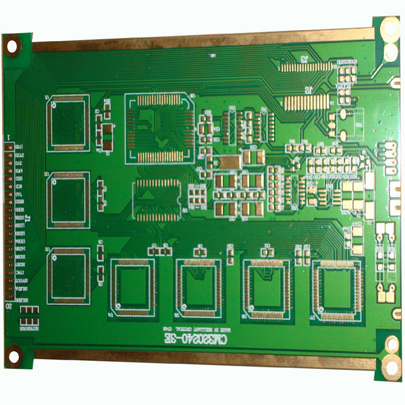
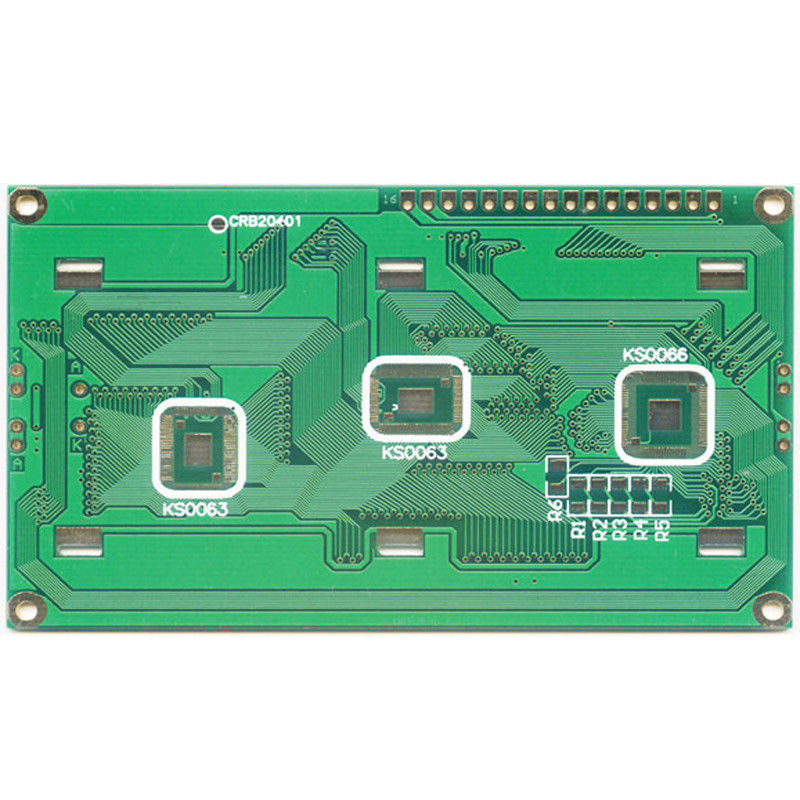
PCB Picture