PCBA design manufacturer SMT components for electronic device
Product Description
|
Product Type |
Al Clad PCB 1 layer~2 layer |
|
Maximum Panel size |
20"*24" (1170mm*600mm) |
|
Copper thickness |
0.5oz, 1oz, 2oz, 3oz and 4 oz |
|
Dielectric Thickness |
0.05mm, 0.075mm, 0.1mm,0.15mm,0.2mm |
|
Substrate Core Thickness |
0.4mm,0.6mm, 0.8mm, 1.0mm, 1.2mm, 1.5mm,2.0mm, 3.0mm and 3.2mm |
|
Finished Board Thickness |
0.4mm To 4.0mm |
|
Thickness Tolerance |
+/-10% |
|
Aluminum Machining |
Drilling,Tapping,Milling,Routing, Die-Punching,break-off tab available |
|
Min. Finish hole size |
0.25mm |
|
Max.working voltage |
2.5kVDC(0.075mm Dielectric), 3.75kVDC (0.15mm Dielectric) |
|
Min.Track Width |
0.2mm (8mils) |
|
Min.Track gap |
0.2mm (8mils) |
|
Min. SMD pad pitch |
0.2mm (8mils) |
|
Surface Finishing |
HASL, HASL Leadfree, Immersion gold, Flash gold, OSP |
|
Soldermask color |
White, Black, others Available |
|
Legend color |
Black, White, others Available |
|
Etest |
YES |
|
Rohs |
YES |
|
Reference Standard |
IPC-A-600G Class 2 |
|
Special holes |
Spot facing, Cup holes |
|
Data Input |
Gerbers, AutoCad, Cam350, PROTEL 99SE,PROTEL DXP, |
OEM/ODM/EMS Services For PCBA
· PCBA, PCB Board assembly: SMT & PTH & BGA
· PCBA and enclosure design
· Components sourcing and purchasing
· Quick prototyping
· Plastic injection molding
· Metal sheet stamping
· Final assembly
· Test: AOI, In-Circuit Test (ICT), Functional Test (FCT)
· Custom clearance for material importing and product exporting
PCB Manufacturing Lead Time
| Layer/Days | Sample(Normal) | Sample(Fast) | Mass Production |
| Single/Double | 2-3days | 24hours | 5-7days |
| Four Layer | 7-10days | 3days | 7-10days |
| Six Layer | 7-10days | 5days | 13-15days |
| Eight Layer | 15-20days | 7days | 15-20days |
PCB Assembly Capabilities
| Turnkey PCBA | PCB+components sourcing+assembly+package |
| Assembly details | SMT and Thru-hole, ISO lines |
| Lead Time | Prototype: 15 work days. Mass order: 20~25 work days |
| Testing on products | Flying Probe Test, X-ray Inspection, AOI Test, functional test |
| Quantity | Min quantity: 1pcs. Prototype, small order, mass order, all OK |
| Files we need | PCB: Gerber files(CAM, PCB, PCBDOC) |
| Components: Bill of Materials(BOM list) | |
| Assembly: Pick-N-Place file | |
| PCB panel Size | Min size: 0.25*0.25 inches(6*6mm) |
| Max size: 20*20 inches(500*500mm) | |
| PCB Solder Type | Water Soluble Solder Paste, RoHS lead free |
| Components details | Passive Down to 0201 size |
| BGA and VFBGA | |
| Leadless Chip Carriers/CSP | |
| Double-sided SMT Assembly | |
| Fine Pitch to 0.8mils | |
| BGA Repair and Reball | |
| Part Removal and Replacement | |
| Component package | Cut Tape,Tube,Reels,Loose Parts |
| PCB assembly process |
Drilling-----Exposure-----Plating-----Etaching & Stripping-----Punching-----Electrical Testing-----SMT-----Wave Soldering-----Assembling-----ICT-----Function Testing-----Temperature & Humidity Testing |
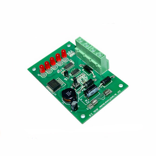
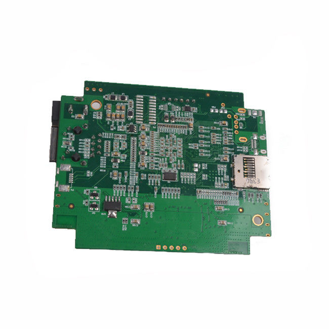
PCBA Picture
![]()
Our products are sold all over the world, you can rest assured.