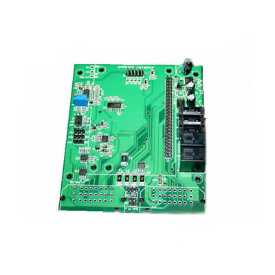

Quality pcb factory for robot vacuum cleaner pcb and pcba assembly
SHINELINK Technology Ltd is a professional PCB manufacturer in China, Shenzhen. With 14 years of development, SHINELINK turns into a first class manufacturer of HDI PCB, with production capability 35,000 square meters. SHINELINK is providing high quality bare PCB and PCB assembly service,including components sourcing, function test,conformal coating and complete assemblyfor clients all over the world.
Our aggressive business strategy enables us to deliver high competitive services for our diverse, competitive customer base. Through this strategy, we are able to make fast, flexible decisions in response to changing market conditions and create most value and benefits for customers.
As for Service, we provide 7-24 on-line professional Pre-sale, Selling and After-Sale service to solve any question about the order. Any time, any requirement will get Prompt Reply from our well-trained and friendly support staff.
Our main market is Europe, north USA,Australia, South America, and Asia. we will put much more effort to build connection with more customers in more area. All we want to do, is to connect the world by our products, to share the Value, Happyness and Achievement with more customers.
OEM/ODM/EMS Services For PCBA
· PCBA, PCB Board assembly: SMT & PTH & BGA
· PCBA and enclosure design
· Components sourcing and purchasing
· Quick prototyping
· Plastic injection molding
· Metal sheet stamping
· Final assembly
· Test: AOI, In-Circuit Test (ICT), Functional Test (FCT)
· Custom clearance for material importing and product exporting
PCB Manufacturing Lead Time
| Layer/Days | Sample(Normal) | Sample(Fast) | Mass Production |
| Single/Double | 2-3days | 24hours | 5-7days |
| Four Layer | 7-10days | 3days | 7-10days |
| Six Layer | 7-10days | 5days | 13-15days |
| Eight Layer | 15-20days | 7days | 15-20days |
PCB Assembly Capabilities
| Turnkey PCBA | PCB+components sourcing+assembly+package |
| Assembly details | SMT and Thru-hole, ISO lines |
| Lead Time | Prototype: 15 work days. Mass order: 20~25 work days |
| Testing on products | Flying Probe Test, X-ray Inspection, AOI Test, functional test |
| Quantity | Min quantity: 1pcs. Prototype, small order, mass order, all OK |
| Files we need | PCB: Gerber files(CAM, PCB, PCBDOC) |
| Components: Bill of Materials(BOM list) | |
| Assembly: Pick-N-Place file | |
| PCB panel Size | Min size: 0.25*0.25 inches(6*6mm) |
| Max size: 20*20 inches(500*500mm) | |
| PCB Solder Type | Water Soluble Solder Paste, RoHS lead free |
| Components details | Passive Down to 0201 size |
| BGA and VFBGA | |
| Leadless Chip Carriers/CSP | |
| Double-sided SMT Assembly | |
| Fine Pitch to 0.8mils | |
| BGA Repair and Reball | |
| Part Removal and Replacement | |
| Component package | Cut Tape,Tube,Reels,Loose Parts |
| PCB assembly process |
Drilling-----Exposure-----Plating-----Etaching & Stripping-----Punching-----Electrical Testing-----SMT-----Wave Soldering-----Assembling-----ICT-----Function Testing-----Temperature & Humidity Testing |
PCBA Picture
![]()