PCB mass production PCB Prototype Printed circuit board manufacture
Welcome to SHINELINK PCB Manufacturer
1. Our Superiority is the Professionalism of our team.
- PCB And PCB Assembly For One-stop Service with Original Components According the BOM.
IC Imported from Digikey / Farnell etc.
- Low Cost with High Quality, Commitment of Quality Assurance.
- For 14 years Experience in PCB Field. ( Our Factory owns advanced production equipment and experienced technical personnel. )
2. Detailed specification of manufaturing capacity
|
NO |
Item |
Craft Capacity |
|
1 |
Layer |
1-30 Layers |
|
2 |
Base Material for PCB |
FR4, CEM-1, TACONIC, Aluminium, High Tg Material, High Frequence ROGERS ,TEFLON, ARLON, Halogen-free Material |
|
3 |
Rang of finish baords Thickness |
0.21-7.0mm |
|
4 |
Max size of finish board |
900MM*900MM |
|
5 |
Minimum Linewidth |
3mil (0.075mm) |
|
6 |
Minimum Line space |
3mil (0.075mm) |
|
7 |
Min space between pad to pad |
3mil (0.075mm) |
|
8 |
Minimum hole diameter |
0.10 mm |
|
9 |
Min bonding pad diameter |
10mil |
|
10 |
Max proportion of drilling hole and board thickness |
1:12.5 |
|
11 |
Minimum linewidth of Idents |
4mil |
|
12 |
Min Height of Idents |
25mil |
|
13 |
Finishing Treatment |
HASL (Tin-Lead Free), ENIG(Immersion Gold), Immersion Silver , Gold Plating (Flash Gold), OSP, etc. |
|
14 |
Soldermask |
Green, White, Red, Yellow, Black, Blue, transparent photosensitive soldermask, Strippable soldermask. |
|
15 |
Minimun thickness of soldermask |
10um |
|
16 |
Color of silk-screen |
White, Black, Yellow ect. |
|
17 |
E-Testing |
100% E-Testing (High Voltage Testing); Flying Probe Testing |
|
18 |
Other test |
ImpedanceTesting,Resistance Testing, Microsection etc., |
|
19 |
Date file format |
GERBER FILE and DRILLING FILE, PROTEL SERIES, PADS2000 SERIES, Powerpcb SERIES, ODB++ |
|
20 |
Special technological requirement |
Blind & Buried Vias and High Thickness copper |
|
21 |
Thickness of Copper |
0.5-14oz (18-490um) |
3. Quote Requirements for PCB and PCB Assembly project
- Gerber File and Bom List;
- Quote Quantity;
- Advise your technical requirements for quoting reference;
- Clearly picturers of PCB or PCB Assembly Sample to us for reference;
- Test Mothod for PCB Assembly.
4. SHINELINK Equipment List
|
NO. |
Machine Name |
QTY |
NO. |
Machine Name |
QTY |
|
1 |
PRESS |
2 |
10 |
Exposurer |
5 |
|
2 |
X-Ray |
1 |
11 |
Deveoloper |
3 |
|
3 |
Brown-Oxidation |
1 |
12 |
Auto V-cut |
1 |
|
4 |
Drilling |
13 |
13 |
AOI |
2 |
|
5 |
Cutter |
1 |
14 |
Routing |
7 |
|
6 |
PTH |
1 |
15 |
ETS |
12 |
|
7 |
PAL |
1 |
16 |
Fly Probe |
4 |
|
8 |
PAT |
1 |
17 |
YAMAHA SMT |
3 |
|
9 |
Flash Gold |
1 |
18 |
FUJI SMT |
4 |
5. PCB and PCB Assembly Lead time
|
Description |
Double side |
Four Layers |
Six Layers |
Above Eight |
HDI |
|
Sample |
4 |
7 |
9 |
9 |
12 |
|
Mass production |
7-9 |
10-12 |
13-15 |
16 |
20 |
|
Assembly |
7-9 |
15 |
16 |
18 |
25 |
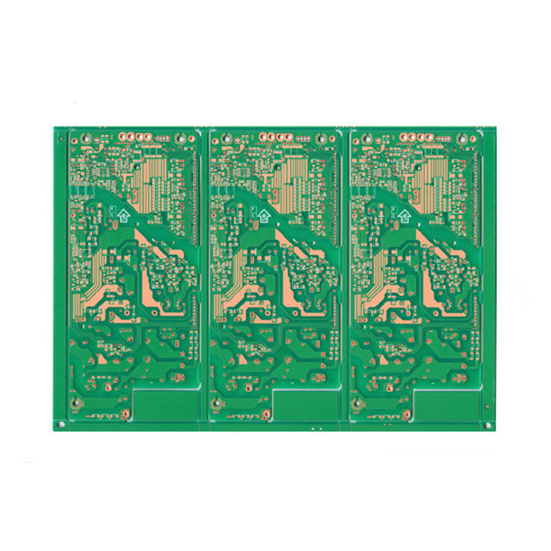
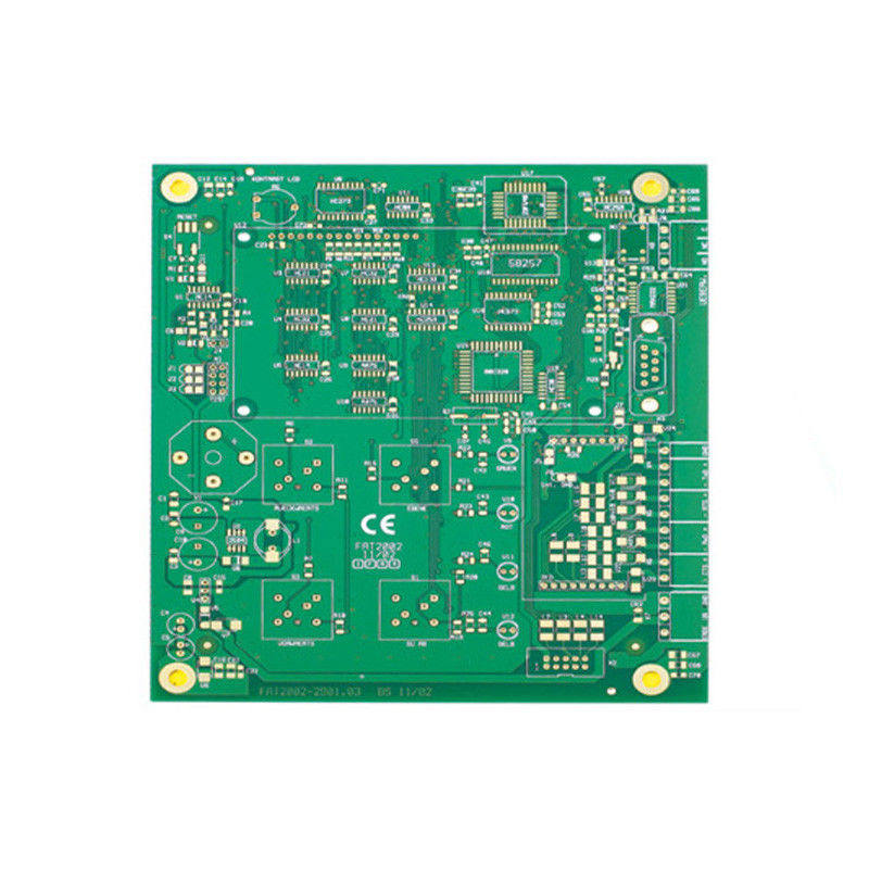
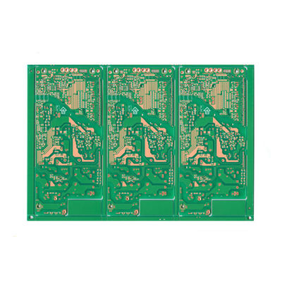
PCB Photo
![]()
Our products are sold all over the world, you can rest assured.