SMT PCB and PCBA Electronic Manufacturing Service for IoT Device
One-Stop Service
1. PCB Copy
2. PCB manufacturing
3. Component sourcing
4. PCB Assembly
5. PCBA 100% test
OEM/ODM/EMS Services For PCBA
· PCBA, PCB Board assembly: SMT & PTH & BGA
· PCBA and enclosure design
· Components sourcing and purchasing
· Quick prototyping
· Plastic injection molding
· Metal sheet stamping
· Final assembly
· Test: AOI, In-Circuit Test (ICT), Functional Test (FCT)
· Custom clearance for material importing and product exporting
PCB Manufacturing Lead Time
| Layer/Days | Sample(Normal) | Sample(Fast) | Mass Production |
| Single/Double | 2-3days | 24hours | 5-7days |
| Four Layer | 7-10days | 3days | 7-10days |
| Six Layer | 7-10days | 5days | 13-15days |
| Eight Layer | 15-20days | 7days | 15-20days |
PCB Assembly Capabilities
| Turnkey PCBA | PCB+components sourcing+assembly+package |
| Assembly details | SMT and Thru-hole, ISO lines |
| Lead Time | Prototype: 15 work days. Mass order: 20~25 work days |
| Testing on products | Flying Probe Test, X-ray Inspection, AOI Test, functional test |
| Quantity | Min quantity: 1pcs. Prototype, small order, mass order, all OK |
| Files we need | PCB: Gerber files(CAM, PCB, PCBDOC) |
| Components: Bill of Materials(BOM list) | |
| Assembly: Pick-N-Place file | |
| PCB panel Size | Min size: 0.25*0.25 inches(6*6mm) |
| Max size: 20*20 inches(500*500mm) | |
| PCB Solder Type | Water Soluble Solder Paste, RoHS lead free |
| Components details | Passive Down to 0201 size |
| BGA and VFBGA | |
| Leadless Chip Carriers/CSP | |
| Double-sided SMT Assembly | |
| Fine Pitch to 0.8mils | |
| BGA Repair and Reball | |
| Part Removal and Replacement | |
| Component package | Cut Tape,Tube,Reels,Loose Parts |
| PCB assembly process |
Drilling-----Exposure-----Plating-----Etaching & Stripping-----Punching-----Electrical Testing-----SMT-----Wave Soldering-----Assembling-----ICT-----Function Testing-----Temperature & Humidity Testing |
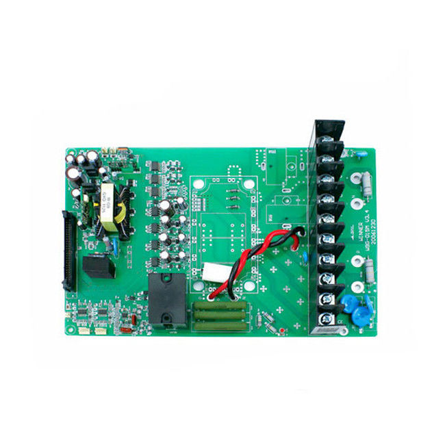
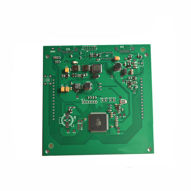
PCBA Picture
![]()
Our products are sold all over the world, you can rest assured.